Posts

Showing posts with the label Wafer Handling

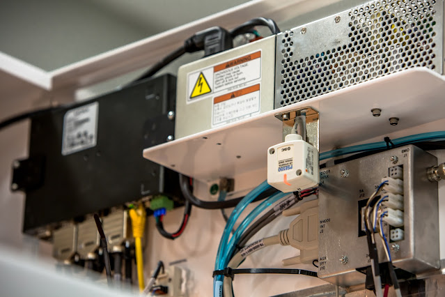
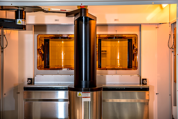
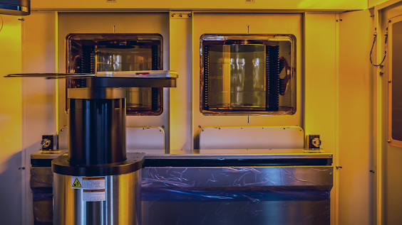
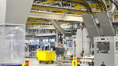
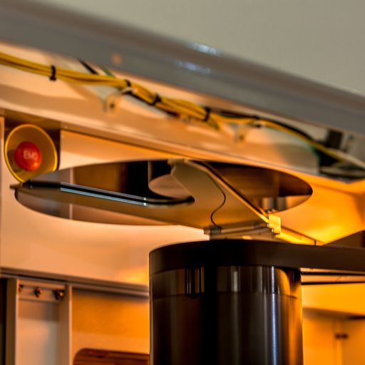
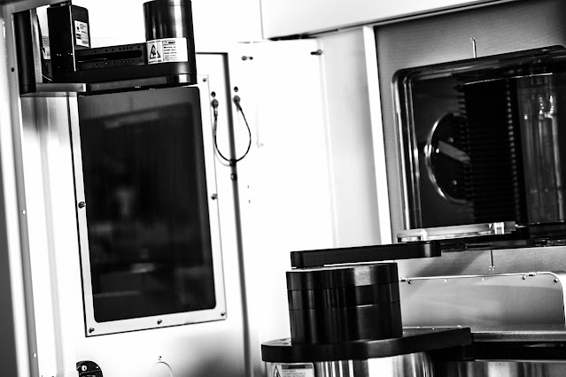
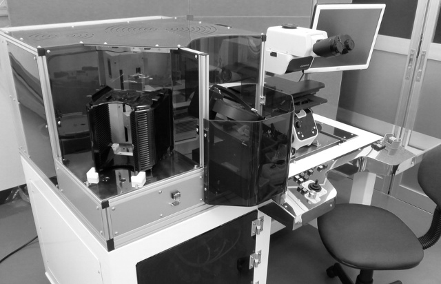
What Are the Advantages of Precision Motion Control?

Image
In the cutting-edge, technologically driven world, precision motion management is critical in several industries, from semiconductor production to robotics. Precision motion control includes the accurate positioning and pressure management of a tool or velocity, often via the use of advanced sensors, actuators, and management algorithms. This technology allows the precise movement and manipulation of items, which is vital in high-tech production procedures and other applications requiring excessive stages of accuracy and repeatability.   Benefits of Precision Motion Control  Enhanced Accuracy and Repeatability  The main advantage of precision movement manipulation is that with this technique, one can achieve excessive accuracy and high repeatability. For instance, in the semiconductor industry, where systems are made of components that are made of particles that can be measured in nanometers, even the smallest variation leads to huge vices and overall system flaws. ...

Essential Role of Front-End Processes in Semiconductor Manufacturing

Image
The front-end processes play a crucial part in creating the silicon chips that power our contemporary gadgets in the complex world of semiconductor production. The purpose of this blog article is to provide insight into the importance of wafer front-end procedures and the crucial processes that turn silicon raw into the intricate integrated circuits (ICs) seen in commonplace gadgets.  Understanding the Semiconductor Front End  The semiconductor front end, commonly referred to as wafer front end or wafer fabrication, refers to the early phases of semiconductor manufacture. Transistors, diodes, and other basic components are made on a silicon wafer using these procedures. The integrated circuit is built on the wafer, and the intricate circuitry that follows is made possible by the front-end operations.   Key Processes in Wafer Front-End Manufacturing  The wafer front end of semiconductor production involves a complex and intricate set of procedures. These process...

Maximizing Yield in 300mm Semiconductor Front End Processes: Critical Role of FOUPs

Image
In the complex world of semiconductor production, where yield optimization at the front-end processes is critical and efficiency is the ultimate goal, the 300mm FOUP (Front Opening Unified Pod) has become a key component. This humble carrier is essential to protecting the fragile wafers that are the foundation of contemporary technology.  Understanding 300mm FOUPs  A 300mm FOUP is essentially a customized container made to move and hold silicon wafers throughout different phases of the production of semiconductor front end. Dust, moisture, and even minute concentrations of chemicals can cause these wafers to become very susceptible to environmental pollutants. The main purpose of the FOUP is to protect these wafers from any damage by offering a hermetically sealed, ultra-clean environment.  Importance of Yield in Front-End Processes  Yield, the percentage of functioning chips generated from a wafer, is an important measure that influences profitability and efficienc...

Wafer Handling Automation Deep Dive: How EFEMs Optimize Semiconductor Manufacturing

Image
In the complex world of semiconductor manufacturing, where efficiency and precision are paramount, automation is essential. The EFEM (Equipment Front End Module), an unsung hero that masterfully controls the smooth transportation and processing of silicon wafers, is at the center of this automation.   In this in-depth analysis, we'll examine the importance of EFEMs, how they improve wafer handling, and their crucial role in the semiconductor industry.  EFEM: Backbone of Wafer Handling Automation  The Equipment Front End Module (EFEM) serves as the choreographer in the complicated ballet of semiconductor manufacture, in which silicon wafers go through transformational procedures. This advanced robotic system serves as the foundation of wafer handling automation, ensuring that wafers travel seamlessly between processing equipment and storage units.  EFEMs use robotic arms, customized carriers, and complex systems to transfer wafers quickly and precisely, reducing...

Future of Semiconductor Manufacturing: How Wafer Handling Automation is Revolutionizing Production

Image
The semiconductor industry is the backbone of modern technology, powering everything from smartphones and laptops to advanced medical devices and autonomous vehicles. As the demand for smaller, faster, and more powerful chips continues to soar, the industry is constantly seeking ways to enhance efficiency, precision, and throughput in manufacturing. One technology that's playing a pivotal role in this evolution is wafer handling automation .  Understanding Wafer Handling Automation  At its core, wafer handling automation involves the use of robotic systems and sophisticated software to manage the movement, processing, and tracking of semiconductor wafers throughout the manufacturing process. Wafers, thin slices of semiconductor material, are the building blocks of integrated circuits (chips). Traditionally, wafer handling was a labor-intensive and error-prone process, but automation has revolutionized it.  Benefits of Wafer Handling Automation  Wafer handling automat...

Optimizing Throughput and Accuracy: Advanced Wafer Automation Techniques

Image
Throughput and accuracy are the two most important factors in the fiercely competitive field of semiconductor production. Accuracy makes sure that the wafers match the industry's strict quality requirements, while throughput defines how many wafers your facility can create in a given amount of time. Wafer automation and sophisticated wafer cassette mapping techniques are useful in this situation.  What is Wafer Automation?  Using specialized robots, equipment, and software to handle and process semiconductor wafers throughout their intricate manufacturing process is known as wafer automation. This has numerous significant benefits over physical labor as it substitutes it at various stages of the process:  Increased Throughput:  Robots and automated systems can operate continuously, significantly boosting the speed of wafer processing.  Enhanced Precision:  Automation reduces the possibility of human mistake, avoiding damage such as scratches or contaminati...

Efficiency in Motion: Wafer Automation with AMAT Robot

Image
In today's ever-evolving semiconductor fabricating era, exactness, speed, and proficiency are fundamental. Not to mention, AMAT Robot combines a high-performance robotization program which is one of the foremost inventive innovations within the industry. Here, in this post, we'll shed light on how these cutting-edge innovations are revolutionizing semiconductor fabricating and driving the industry forward.   The Semiconductor Manufacturing Challenge    Semiconductor manufacture could be a complicated handle that requires exactness at all stages. From wafer stacking and emptying to review and pressing, each prepare must be completed immaculately. Truly, these operations were as often as possible labor-intensive, time-consuming, and vulnerable to human botch. Find the world of AMAT Robot and Wafer automation.   Precision and Efficiency in AMAT Robots    Wafer-handling robots are the mainstays of semiconductor production. These specialist robots are...

Efficiency Unleashed: The Power of Wafer Automation!

Image
Every faultless execution or cutting-edge technological development conceals an entire realm of precision and ingenuity that is frequently unavailable to the general audience. The undiscovered treasures of semiconductor manufacturing are the labs dedicated to wafer automation and stage repair . This article will examine the fascinating features of these particular labs, where expertise and advances in technology combine to create immaculate environments and progress within the semiconductor industry.    Phases of Creation and Replication: The Alchemy of Substances    Professional stage repair services are often not exposed to threats and are a more reliable option, especially for critical applications where precision is non-negotiable. Like wizards, the skilled workers fuse elements and wisdom to create fresh possibilities for semiconductor manufacturing. Whether it's by restoring modern semiconductor companies or reconstructing antique instruments, something extraor...

Unveiling the Wonders of Kensington Controllers and Wafer Handling!

Image
There is no denying the fact that Wafer handling and Kensington controller are two hidden icons that are crucial to the constantly changing fields of precision engineering and technology. These humble parts are the foundation of state-of-the-art systems, quietly changing the way we use technology. Let's investigate the world of these technical wonders and discover all the advantages they provide.   Kensington Controllers: A Symphony of Control and Precision  Kensington controllers' inventiveness is the key to flawless user experiences. These often-ignored gadgets are the maestros arranging the control symphony in a variety of electronic applications. a Kensington controller offers an easy-to-use interface that improves user engagement with unprecedented precision on a variety of devices, including smart gadgets and arcade machines.   Enhanced Ergonomics for Unmatched Comfort   The dedication of a Kensington controller to ergonomics is one of their mos...

Beyond the Surface: Exploring the Science Behind Wafer Handling Robots

Image
Wafer Handling Robots are the unsung heroes in the dynamic world of semiconductor fabrication, helping the complex dance of silicon wafers. It becomes increasingly important for business leaders to comprehend the subtleties of the Wafer front end as they dive deeper into cutting-edge technologies. By dissecting the science underlying their functionality and highlighting their crucial position in the semiconductor industry, this blog seeks to clarify the significance of wafer-handling robots .  The Beginning of Precision: A Look into Wafer Front End Fundamentals   The Wafer front end, a crucial stage that establishes accuracy and dependability, is at the center of semiconductor production. Wafers are loaded onto the production line and undergo an initial inspection, among other procedures, at this step. Business owners who are eager to streamline their manufacturing procedures need to understand how important this initial phase is to guarantee the caliber of the finished s...

Transforming Semiconductor Production: The AMAT Automaton and the Wafer Front End

Image
The AMAT Robot is an innovative technological marvel at the cutting edge of accuracy and effectiveness in the complex field of semiconductor production. Here, in this post, we'll delve into the intricacies of the wafer front-end process, as well as examine how the AMAT Robot is revolutionizing the semiconductor sector.   Understanding the AMAT Robot: The Mind Behind the Operation    The AMAT Robot is a silent force that performs unparalleled precision in orchestrating intricate processes at the center of semiconductor manufacturing. With its ability to maneuver through the intricacies of the front end with ease and guarantee the highest productivity in semiconductor creation, this robotic stronghold has wholly changed the wafer processing setting.   Redefining Precision: Handling the Wafer Front End    The wafer front-end process in the semiconductor manufacturing industry is like a finely choreographed movement of tiny parts. The AMAT Robot expe...

Transforming Semiconductor Production: The Hidden Wonders of Automation and Wafer Handling!

Image
In the complex realm of semiconductor manufacturing, wherein consistency is critical, wafer handling and automation systems are crucial. Wafer handling becomes a key role in this technical ballet, directing an intricate symphony of wafer movement with unmatched dexterity. Here, in this post, we will shed light on the expanse of automation and wafer handling, discovering the mysteries that drive the digital revolution.   The Harmony of Wafer Management: An Introduction to Accuracy   Wafer handling is a symphony of accuracy executed in maze-like semiconductor production facilities. Wafer transportation is a demanding operation that involves moving wafers from one stage to another precisely timed like a work of art. With the dexterity of a surgeon's knife, automated guided vehicles (AGVs) softly traverse cleanroom conditions while transporting these wafer-thin disks. The pristine condition of these tiny silicon canvases is protected by the motion of automation, which g...

Unveiling the Intricacies of Wafer Front End in Semiconductor Manufacturing

Image
The digital era is powered by semiconductor technology, which is transforming our environment through intricate yet necessary procedures. The wafer front end , a critical component in the production of semiconductors, is at the center of this technological marvel. Comprehending this essential procedure is essential to appreciating how technology powers our gadgets and systems created.  Investigating Wafer Front End   The term "wafer front end" in the context of semiconductor manufacturing describes the first stage of building the integrated circuits that serve as the foundation for electronic devices. A number of complex procedures are involved in this phase, which lays the foundation for the entire semiconductor manufacturing process.  What is the Wafer Front End?   The wafer front end primarily encompasses three key stages: wafer preparation, wafer fabrication, and wafer testing.  Wafer Preparation: In this initial step, silicon wafers are prepared. ...

Elevating Semiconductor Manufacturing: The Crucial Role of Wafer Handling and Cassette Mapping!

Image
In the complex world of semiconductor manufacturing, control and precision are critical. The uninitiated may frequently overlook two important facets of this industry, but they are vital to the production process: wafer handling and wafer cassette mapping. These unnoticed luminaries operate tenaciously to guarantee that the highest quality standards are fulfilled in the production of every chip. In this post, we will examine the depths of these procedures, as well as their importance, subtleties, and smooth interaction with one another.   Wafer Handling: The Basis    The foundation of semiconductor manufacturing is wafer handling. Wafers are moved, transported, and positioned during different stages of the production process. Cited below are some attributes that highlight its significance:   Immaculate Hygiene    Handling wafers takes place in highly regulated spaces known as cleanrooms. Semiconductor devices can be destroyed by contaminants, eve...

Wafer Handling Robot and EFEM: Enhancing Semiconductor Performance

Image
 A wafer-handling robot is a robotics system that automates the handling of silicon wafers during the manufacturing process of semiconductors. Several tasks are executed by the wafer-handling robots , such as cassette mapping, wafer distribution, and wafer tilt check. These are highly beneficial in lessening adulteration during wafer processing. Nevertheless, they demand a high initial acquisition.    Applications of wafer-handling robots  In unified circuit manufacturing, a wafer-handling robot moves and adjusts wafers. These facilitate the rate of product flaws by pushing products quickly and in a way that is correct in all details.   These are very common in the industrial sector and can be used to:  Move materials from one workstation to another.   Select, style, package, and palletize products.   Push parts and elements from one assembly line to another.  Deliver a part to a welding robot.   Transm...

All You Need to Know About Handling Robot Surge!

Image
 Are you considering automating your material handling or logistical procedures with robotics?  Many businesses are deploying more accessible, adaptable, and quick robots to streamline operations for machine tending, part transfer, assembly, picking, packaging, palletizing, and other tasks to remain competitive. So much so that, of all the automated material handling equipment, robots had the most significant market size in 2020.   Driving Reasons for Material Handling Robot Growth   Although the usage of semiconductor robot handling equipment has historically helped increase operational effectiveness, enhance product quality, and lower production costs, there are now more modern, diverse reasons motivating firm executives to adopt them.   Shifting Consumer Behavior   Large production runs in low-mix manufacturing environments continue to occur. Still, as customer needs become more complicated, production methods must be more flexible t...

Motion Control Solutions for the Semiconductor Manufacturing Sector

Image
 When Intel created its first microchips, nanometer accuracy wasn't really needed. In contrast to modern 10 nanometers and smaller structures, the Intel 4004 processor's structure widths in 1971 were a generous 10 microns or 1/100 of a millimeter. On a 1-dimensional scale, that is 1,000 times more minor, but on a planar scale, it is 1,000,000,000 times larger. Moore's law, which governs this shrinkage process, states that the number of electronic circuits must double every 18 months.    Recent advancements in performance and power consumption due to the combination of photonics and electronics are significant when considering the environmental impact of the massive server farms necessary for cloud computing and Big Data applications. Miniaturization of semiconductor components essentially combines the benefits of speed, cost, economy, and reliability; higher integration results in fewer discrete components and, thus, a lower failure risk.   The visionary functio...

How the Right Wafer Handling End-Effector Boosts Robotic Productivity?

Image
End effectors are necessary for manipulators and robotic arms to accomplish their intended functions. They allow wafer handling end effector to engage with a subject by attaching to manipulator arms or a robot's wrist. These parts are perfect for assembly, pick-and-place, and machine-tending applications because operators frequently use gripper end effectors to raise and handle specific objects using robotic machinery. End effectors for robotics or manipulators are used in operations to enhance safety protocols or eliminate any worries about using this equipment.   Types of End-Effectors   Depending on the intended application, operations may use various end effectors to carry out specific duties.   Robotic Process Tools   Robotic Welding: Robot arms with welding end effectors, which are most frequently used in the automotive sector, are commonly used in applications. Robotic welding systems typically deliver excellent outcomes due to their accur...

Integration of Wafer Handler into a Fully Automated Probe Station!

Image
Before delving further into that, let's check what completely automatic probe stations and wafer handlers are. It might be challenging to integrate wafer handlers to construct a completely automated probe station; therefore, having a fundamental understanding of the procedure is quite beneficial. And if you are seeking the best AMAT robot, feel free to contact Kensington Labs. Wafer handling automation Fully Automated Probe Station A wafer handler, also known as a robot or material handling unit, and pattern recognition software, also known as auto-alignment, are commonly included in fully automated probe stations. Wafer Handler The material handling part of the probe system is called a wafer handler (MHU). A pre-aligner, a robot with an end-effector (paddle), cassette holders (1 or 2), a robot with an end-effector enclosure, and a safety/environmental enclosure are commonly included. It is integrated with the probe. Wafer handlers can frequently work with a wide range of wafe...