Wafer Handling Robots Proves Advantageous In Various Fields
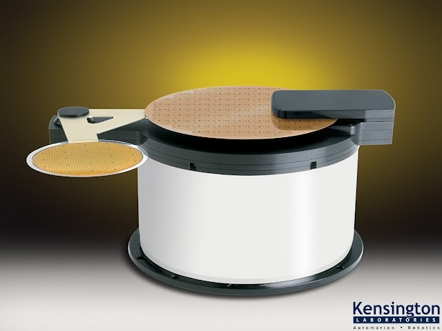
Semiconductor equipment has a huge burden of equipment front-end module designs which result in less tool productivity. Without doubt, semiconductor manufacturing spans various stages and is a complex process. A huge emphasis is laid upon cost as well as quality in semiconductor equipment. 300mm FOUP proves effective in various wafer mapping procedures. Wafer handling robots are best in the business as they offer accuracy as well as repeatability. In manual wafer handling, there is an increased workload which can only be solved by Wafer handling robots. Wafer handling robots provide a logical approach to decrease the manual workload. Current wafer handling robots can pick and place 300mm wafers in a sequence in a repeated manner. Wafers are picked and placed based on the location of the joint. A typical sequence involves • Extend to wafer pick location • Pick wafer • Retract to a safe po...