Wafer Handling Robots Proves Advantageous In Various Fields
Semiconductor equipment has a huge burden of equipment
front-end module designs which result in less tool productivity. Without doubt,
semiconductor manufacturing spans various stages and is a complex process. A
huge emphasis is laid upon cost as well as quality in semiconductor equipment.
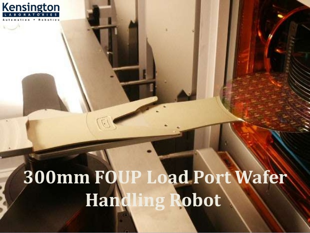
300mm FOUP proves effective in various wafer mapping procedures.
Wafer handling robots are best in the business as they offer
accuracy as well as repeatability. In manual wafer handling, there is an
increased workload which can only be solved by Wafer handling robots. Wafer
handling robots provide a logical approach to decrease the manual workload.
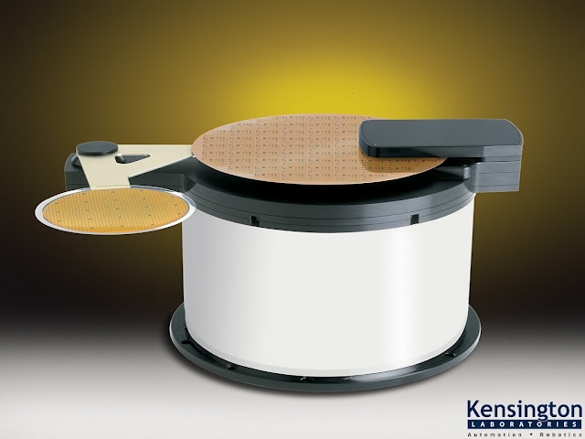
Current wafer handling robots can pick and place 300mm
wafers in a sequence in a repeated manner. Wafers are picked and placed based
on the location of the joint. A typical sequence involves
• Extend to wafer
pick location
• Pick wafer
• Retract to a safe
position
• Extend arm to
place location
• Place wafer
• Repeat
Tasks are performed in a series by a wafer handling robots
to make sure the robot has reached the point where it has been directed to go.
To increase the output, the main focus of robot manufacturers is to decrease
the time consumed in each process.
Features Of Wafer Handling Robots
Wafer handling robots complete the task in an efficient
manner which otherwise consumes plenty of time manually. They are extremely
precise and have the ability to complete the task in minimum time. By
monitoring the electrical overhead and by safety scanning, collisions are
avoided.
Wafer handling robots have observed significant
advancements- high throughput and superior performance are some of the features
which make wafer handling robots a favorite of manufacturing firms.
The commands are fairly easy to learn; with some research,
they can be self-learned. These robots are equipped to identify fault and
recovery which make them a preferred choice of the industries.
Wafer mapping sensors are trouble-free to maintain, easy and
safe to use. They reduce the manufacturing cost significantly as they improve
efficiency. The assimilated barcode reader or the off-axis reader along with
the direct optical algorithm of the entire involved axis tends to the
recurrence of wafer placement. This trait makes wafer mapping one of the best in the competition. To analyze data
wafer handling software is widely used.
300mm FOUP offers a robust design and
amazing sealing capability. It offers secure and clean wafer transport,
integration and optimum automation at an effective cost. To analyze data wafer
handling software is widely used.


Comments
Post a Comment