Posts

Showing posts from April, 2022

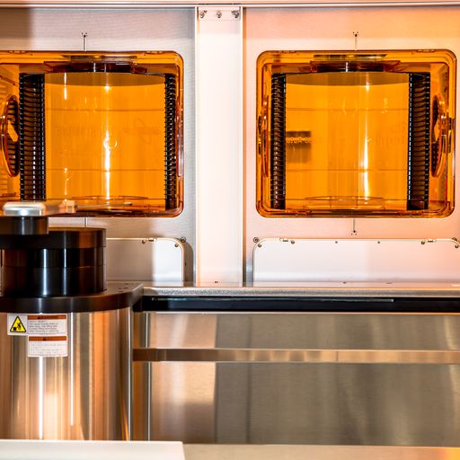
Find the Defects on a Wafer with Advanced Semiconductor Wafer Defect Inspection System

Image
The semiconductor sector is mainly engaging in designing as well as fabrication of semiconductors . It has been analyzed that the automation sector is in great demand for the entire electronics manufacturing industry. There are many professionals who provide the best wafer stage solutions . So, you must rely on the best experts that will meet your exact demands.    When it comes to precision linear & rotary positioning stages, the semiconductor wafer inspection sector needs high precision. Metrology as well as inspection are considered the two essential terms used for the management of the semiconductor manufacturing process.     There are approx. hundreds of steps involved in the overall manufacturing process of semiconductor wafers which, of course, takes a lot of time. If any defects occur early in the manufacturing process, all the work undertaken to perform the steps will be wasted. That is why metrology & inspection processes must be established at critical points of

A Quick Walkthrough about the Changing Wafer Size & the Move to 300mm

Image
Technology is transforming rapidly, and so is the semiconductor sector. Recent advancements had a great influence on the semiconductor production process. The industry’s ability to increase productivity by 25-30 percent every year is the combined result of wafer size transitions, equipment productivity improvements, shrinking device geometries, as well as incremental yield modifications. In fact, the Wafer size transitions account for 4 percent of the 25-30 % productivity profit. Do you want to buy Foup opener for your business? Try Kensington Labs equipment, and you will surely get satisfactory results.    Companies make wafer size transitions because of the overall benefits in terms of cost resulting from the larger number of dice per wafer, thus using the same number of process steps in order to produce more dice. Based on the latest trends, nowadays, there is peak demand for 300mm. By 2000, the first processing of 300mm (12 inches) wafers is anticipated. The 300mm wafers will acc