A Quick Walkthrough about the Changing Wafer Size & the Move to 300mm
Technology is transforming rapidly, and so is the semiconductor sector. Recent advancements had a great influence on the semiconductor production process. The industry’s ability to increase productivity by 25-30 percent every year is the combined result of wafer size transitions, equipment productivity improvements, shrinking device geometries, as well as incremental yield modifications. In fact, the Wafer size transitions account for 4 percent of the 25-30 % productivity profit. Do you want to buy Foup opener for your business? Try Kensington Labs equipment, and you will surely get satisfactory results.
Companies make wafer size transitions because of the overall benefits in terms of cost resulting from the larger number of dice per wafer, thus using the same number of process steps in order to produce more dice. Based on the latest trends, nowadays, there is peak demand for 300mm. By 2000, the first processing of 300mm (12 inches) wafers is anticipated. The 300mm wafers will accommodate roughly twice as many dice per wafer as 200mm wafers.
Many companies have already upgraded to a new wafer size. Interestingly this move seems to be beneficial. Beyond 300mm, it jumps to 450mm wafers. Many companies around the globe manufacture semiconductor equipment and provide the best repair services, but the services provided by the Kensington labs are unmatched.
Get in touch with the Kensington labs experts if you want to buy a 300mm load port.
Viewpoint for 300mm Wafer Processing
Perhaps the major question in 300mm development concerns the cost problem – How will the semiconductor manufacturing & equipment, and materials suppliers, with combined market size of approx. $170 billion, build a $15-20 billion infrastructure for 300mm processing in some years while meeting ongoing needs for device & process development for 0.25µm, 0.18µm, as well as future generations of devices?
Probably most semiconductor manufacturers will find that through the alternative device design techniques, a smaller die size can be possible, thereby delaying the 300mm adoption out to the 0.15µm or 0.13µm generation. Moreover, the information from SEMI shows that standards will be jointly developed, but the tool projects are separate efforts.
The companies will carefully observe all the advantages & disadvantages related to the 300mm transition. No one in the industry can predict how many companies will use these larger wafers. This, of course, is because the number of manufacturers has never needed to progress beyond 150, 125, or even 100mm wafer processing. But in the present era, everyone wants to join hands with the new technology. Thus, the wafer size transitions will make things more cost-effective, especially the move to 300mm and maybe 450mm.
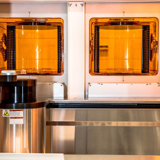
About Kensington Labs
Kensington Labs is a leading robotics and automation solutions provider that enables semiconductor manufacturers to increase manufacturing productivity. Kensington being your wafer handling robot and precision motion control partner, you get the best wafer handling robot solutions, precision motion control solutions, new products tailored to particular needs for wafer handling robots, as well as precision motion control applications. They possess an excellent spares & repairs program. The company offers an Automatic Door Opener™ (ADO) – FOUP Load Port with proven HVM wafer handling performance. Talk with the experts to get the best services. For more details regarding the 300mm foup, you may refer to the website.


Comments
Post a Comment