Posts

Showing posts from June, 2023

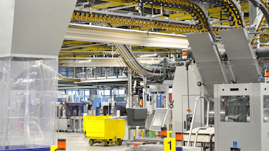
All You Need to Know About Handling Robot Surge!

Image
 Are you considering automating your material handling or logistical procedures with robotics?  Many businesses are deploying more accessible, adaptable, and quick robots to streamline operations for machine tending, part transfer, assembly, picking, packaging, palletizing, and other tasks to remain competitive. So much so that, of all the automated material handling equipment, robots had the most significant market size in 2020.   Driving Reasons for Material Handling Robot Growth   Although the usage of semiconductor robot handling equipment has historically helped increase operational effectiveness, enhance product quality, and lower production costs, there are now more modern, diverse reasons motivating firm executives to adopt them.   Shifting Consumer Behavior   Large production runs in low-mix manufacturing environments continue to occur. Still, as customer needs become more complicated, production methods must be more flexible to allow product modification and personalization.

Semiconductor Front End Manufacturing: Challenges, and Enhancement!

Image
A step in producing semiconductors is referred to as semiconductor front-end manufacturing. Every semiconductor electronic component, including the microcontroller, logic ICs, and even basic MOSFET transistors, must go through several production steps before being supplied with recognizable form factors. Wafer fabrication and probing are semiconductor front end manufacturing, whereas wafer cutting, assembly, and packaging are back-end electronics manufacturing processes. Then, the semiconductors adopt QFP, SOP, SOIC, and other typical form factors utilized in PCB design.  Doping the semiconductor wafer is the first step in front-end electronics fabrication in semiconductor manufacturers. As a result of this process, some insulative silicon portions become conductive areas. Diffusion is adding doping gases to the silicon die in a furnace. Alternately, ionic implantation can dope silicon dies by directing an electron beam at them. Additionally, the silicon dies to go through a photo mas

Motion Control Solutions for the Semiconductor Manufacturing Sector

Image
 When Intel created its first microchips, nanometer accuracy wasn't really needed. In contrast to modern 10 nanometers and smaller structures, the Intel 4004 processor's structure widths in 1971 were a generous 10 microns or 1/100 of a millimeter. On a 1-dimensional scale, that is 1,000 times more minor, but on a planar scale, it is 1,000,000,000 times larger. Moore's law, which governs this shrinkage process, states that the number of electronic circuits must double every 18 months.    Recent advancements in performance and power consumption due to the combination of photonics and electronics are significant when considering the environmental impact of the massive server farms necessary for cloud computing and Big Data applications. Miniaturization of semiconductor components essentially combines the benefits of speed, cost, economy, and reliability; higher integration results in fewer discrete components and, thus, a lower failure risk.   The visionary functionalities of