Motion Control Solutions for the Semiconductor Manufacturing Sector
When Intel created its first microchips, nanometer accuracy wasn't really needed. In contrast to modern 10 nanometers and smaller structures, the Intel 4004 processor's structure widths in 1971 were a generous 10 microns or 1/100 of a millimeter. On a 1-dimensional scale, that is 1,000 times more minor, but on a planar scale, it is 1,000,000,000 times larger. Moore's law, which governs this shrinkage process, states that the number of electronic circuits must double every 18 months.
Recent advancements in performance and power consumption due to the combination of photonics and electronics are significant when considering the environmental impact of the massive server farms necessary for cloud computing and Big Data applications. Miniaturization of semiconductor components essentially combines the benefits of speed, cost, economy, and reliability; higher integration results in fewer discrete components and, thus, a lower failure risk.
The visionary functionalities of wafer handling tools, stage repair, precision control systems, and wafer cassette mapping are the end-to-end solutions to raise the performance of the semiconductor.
Precision Motion, Nanopositioning, and Alignment Solutions for Extremely Sensitive Manufacturing Processes
The production and inspection processes for semiconductors are very demanding and delicate. The process begins with pulling the monocrystalline ingot and lasts until the finished chip is contacted and finally packaged. Modern nanolithography is essential for miniaturization. Modern laser sources are used in the exposure process to design the structures for conductor tracks, transistors, and other functional parts on the unprocessed silicon wafer. Extreme precision, equipment, and conditions are needed when working with nanometer-sized features:
The limits of what is theoretically possible are being pushed further from chip generation to chip generation. Examples include:
- Maximum cleanliness.
- Sharp-edged imaging of incredibly small structures.
- Highly dynamic, coordinated movements of masks and wafers in the lithography equipment.
Additionally, nanopositioning technology has long proven useful. If you are looking for the best XYZ precision stage solution, Kensington Laboratories is the one-stop solution.
Involved in Different Process Steps
Apart from nanolithography, precision motion stages and subsystems are used in various additional process steps, in manufacturing semiconductor components. And it is actively advancing the semiconductor industry from the bottom up, beginning with creating sub-floor platforms and tool structures that utilize the most cutting-edge vibration-canceling technology.
Laser beam steering tip/tilt systems were created to deliver exact beams, combining Canadian resolution with quick millisecond scale reaction and settling. New patented technology enables ceramic shims to be programmed to change dimensions in the nanometer range to correct for errors that develop over time or with temperature changes. This set-and-forget technology can easily make changes to the alignment of optical systems or huge mechanical assemblies.
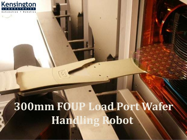
Kensington is a renowned supplier of wafer handling robots, precision motion control, and linear, rotary, and integrated stages designed to fulfill the most challenging needs.


Comments
Post a Comment