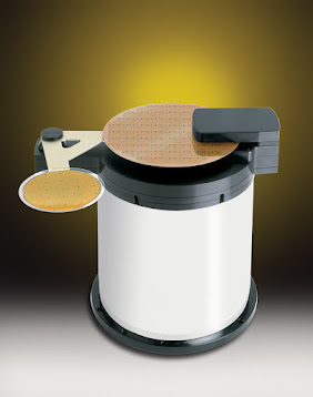
Unleash The Top Features Of Wafer Mapping Sensors

Wafer mapping sensors have gained popularity to detect slotting errors in semiconductor wafers. Proper setup of the wafer mapping sensor should be done, and wiring, alignment, and operation should be taken care of. Wafer mapping sensors have gained popularity to detect slotting errors in semiconductor wafers. Usually, it is mounted on wafer handling devices or robot arms, and it also has a broad range of mapping applications. These sensors are used for notching or flattening the various wafer sizes. However, they cannot be used in the presence of dark, ultra-thin wafers. Main features of wafer mapping sensors Ultra-fast response and non-intrusive wafer mapping solution protects the wafer front end from inadvertent crashes Sensors work on digital signal processing logic to know about the size or edge geometry, The direct interface does amplification or signal conditioning This economical sensor even detects dummy wafers and has remote teaching capability which results in reduced downtim...