Unleash The Top Features Of Wafer Mapping Sensors
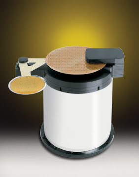
Wafer mapping sensors have gained popularity to detect slotting errors in semiconductor wafers. Proper setup of the wafer mapping sensor should be done, and wiring, alignment, and operation should be taken care of.
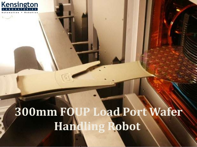
Wafer mapping sensors have gained popularity to detect slotting errors in semiconductor wafers. Usually, it is mounted on wafer handling devices or robot arms, and it also has a broad range of mapping applications. These sensors are used for notching or flattening the various wafer sizes. However, they cannot be used in the presence of dark, ultra-thin wafers.
Main features of wafer mapping sensors
- Ultra-fast response and non-intrusive wafer mapping solution protects the wafer front end from inadvertent crashes
- Sensors work on digital signal processing logic to know about the size or edge geometry,
- The direct interface does amplification or signal conditioning
- This economical sensor even detects dummy wafers and has remote teaching capability which results in reduced downtime
- Wafer cassette mapping is done with both silicon wafers and glass wafers
- It is frequently used for testing coating and tolerances
- Easy adjustments within a minimal time fasten the teaching function
Proper setup of the wafer mapping sensor should be done, and wiring, alignment, and operation should be taken care of.
During wafer mapping, a sensor is used to move a wafer carrier from the first wafer to the one sensor beyond the last slot. The scans always minimize sensor latency, mechanical backlash, and sensor hysteresis effects.
The sensor can detect wafers of all sizes, thicknesses, irrespective of their coating types. In some cases, one needs to adjust the sensitivity. There are sensors with the ambient-light filter that are used for blocking visibility and infrared light from the phototransistor and high-pass filter.
The wafer mapping sensors are always used for optimum performance during operation. The sensors face the wafer to make the working angle zero for scanning the wafer edge at different points for redundancy and to detect wafer tilt or find any misplaced wafer. They also check the flatted wafers used for a wide working angle range. The wafers scan strategy is used to see the orientation, and to recommend the best working angle of the sensor. Generally, two scans are used to scan the suggested working angle. When the sensor is mounted on a wafer handling robot, the sensor working angle should not be confused with the robot arm angle.
How To Calculate The Distance?
Distance from the wafer to the sensor is set at the optimum detecting distance, to ensure sensors perform satisfactorily in the specified maximum detecting range. They are calculated to achieve the best performance at the specified optimum detecting distance.
The experts recommend using wafer mapping sensors within the specified maximum detecting range to match and respond to wafers throughout carefully.
When it is outside the specified range, the sensor response degrades, so it always makes it in the full possible range of wafer parameters. Even if it responds correctly to a test wafer, there are other distances at which the sensor will not respond correctly to all wafers.
Sensors only detect all standard notched and flatted wafers for robust detection and even if there is a misalignment in the setup. In the scans, the sensors correctly detect the wafer seen on only one of the two scans. Wafer front end sensors are used to identify flatted wafers with multiple scans. Check the working angle specifications while calculating the exact number and positions of scans required scanning properly.
Wafer cassette mapping sensors are the main components of the wafer mapping system, and they impact the robustness of wafer detection broadly. For detecting cross-slotted or ultra-thin wafers, sensors need a dynamic range of wafer coatings to make sure everything in the optimal wafer maps is achieved.
Source:- https://bit.ly/31hz8Sg


Comments
Post a Comment