Posts

Showing posts with the label Kensington Laboratories

Future of Semiconductor Manufacturing: How Wafer Handling Automation is Revolutionizing Production

Image
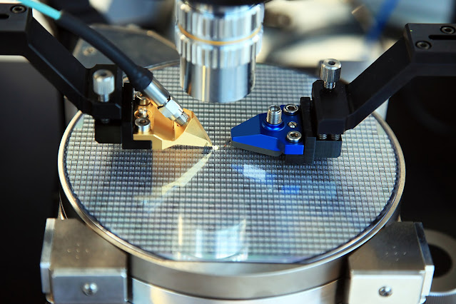
The semiconductor industry is the backbone of modern technology, powering everything from smartphones and laptops to advanced medical devices and autonomous vehicles. As the demand for smaller, faster, and more powerful chips continues to soar, the industry is constantly seeking ways to enhance efficiency, precision, and throughput in manufacturing. One technology that's playing a pivotal role in this evolution is wafer handling automation .  Understanding Wafer Handling Automation  At its core, wafer handling automation involves the use of robotic systems and sophisticated software to manage the movement, processing, and tracking of semiconductor wafers throughout the manufacturing process. Wafers, thin slices of semiconductor material, are the building blocks of integrated circuits (chips). Traditionally, wafer handling was a labor-intensive and error-prone process, but automation has revolutionized it.  Benefits of Wafer Handling Automation  Wafer handling automat...

Optimizing AMAT Robot Performance: A Guide to Precision Motion Control Techniques

Image
Precision is critical for success in the highly competitive and challenging sector of semiconductor production. Applied Materials (AMAT) robots are a hallmark of this industry, noted for their dependability and ability to handle delicate wafers with pinpoint precision. Even the best robotic systems might benefit from tuning to guarantee they continue to function at optimal levels.  This article looks into crucial precision motion control techniques for maximizing the capabilities of your AMAT robot.  Understanding Precision Motion Control  Precision motion control lies at the heart of manufacturing processes that demand accuracy and repeatability - nowhere more so than in semiconductor production where AMAT robots excel. This form of motion control goes beyond simple movement. Here's what it entails:  Accuracy: The ability of the robot to reach the exact intended position within tight tolerances, often measured in microns.  Repeatability: The robot's capacity...

Wafer Cassette Mapping: The Essentials for Semiconductor Manufacturing

Image
In the complex world of semiconductor production, efficiency and precision are not just desirable outcomes, but rather requirements. Every tiny transistor that is etched into a silicon wafer needs to be precise since any mistake might result in expensive losses.  Here's where wafer cassette mapping comes into play: it's the foundation of quality control that protects yield and guarantees the creation of perfect electronics.   What is Wafer Cassette Mapping?  Let's begin by envisioning the procedure. Semiconductor manufacturing starts off with pristine silicon wafers, which are tiny, round discs that serve as the basis for integrated circuits. These wafers are housed in protective containers called cassettes. Wafer cassette mapping is the process of meticulously analyzing each wafer within a cassette, pinpointing defects, identifying performance variations, and classifying the individual dies. This mapping process generates a visual representation of the wafer – a "m...

Precision and Speed: Optimizing Wafer Automation with Advanced EFEMs

Image
Semiconductor manufacturing – the backbone of the modern digital world – operates on a microscopic scale. The slightest deviation in the fabrication of delicate silicon wafers can compromise the performance and yield of countless electronic devices.   As the insatiable demand for greater computing power and smaller form factors intensifies, optimizing speed and absolute precision during wafer handling has become critical. Let's explore how advanced EFEMs are pushing the boundaries of precision and speed in wafer automation .  What is an EFEM?  An EFEM (Equipment Front-End Module) is the entrance point for wafers into advanced semiconductor manufacturing machines. It functions as a tightly regulated mini-environment, protecting delicate wafers from contamination while maintaining ideal atmospheric conditions during loading, unloading, and temporary storage.  EFEMs work in perfect synergy with wafer-handling robots or automated material handling systems (AMHS) ens...

Managing the Peak of Accuracy: Unveiling the XYZ Precision Stage and Wafer Stage Wonders

Image
Two unnoticed luminaries take the forefront in the complex world of precision engineering: the Wafer Stage and the XYZ Precision Stage. Here, in this post, we will shed light on the unique benefits each step offers and the important things to consider when selecting the best equipment for your accuracy requirements.   The XYZ Precision Stage: A precise symphony created by the convergence of three axes    Imagine a performance in which the smooth harmonization of three axes produces a precision symphony. It is what makes the XYZ Precision Stage so appealing. The X, Y, and Z axes all function independently to enable complex movements with unmatched precision. This stage is an example of the pinnacle of precise engineering, whether it comes to intricate movements or microscopic modifications.   A Movement of Wafer Manipulation: The Wafer Stage Waltz    The Wafer Stage is the phase where wafer manipulation transforms into a creative medium. With its ...

Mastering Precision: Motion Control and Wafer Cassette Mapping

Image
There is no denying that accuracy is paramount as well as the basis for enhancing the intricate sector of semiconductor fabrication. Moreover, upholding accurate action management is necessary in order to unlock unmatched effectiveness and productivity in the ever-evolving realm of robotics. In addition to this, wafer cassette mapping is essential in the semiconductor front end, where silicon wafers are converted into elements of electronic phenomena. Consider it a complex map reliably directing every wafer via a maze of procedures. Here, in this post, we will shed light on the intriguing sector of precision motion control , focusing on ground-breaking wafer cassette mapping.   Precision Motion Control: What to know  Explaining the precision motion control, the name itself signifies the enigma itself. It deals with the meticulous management of movement in various mechanical systems. It is the skill of conforming to authentic positioning, pace, and synchronization to creat...

Beyond the Surface: Exploring the Science Behind Wafer Handling Robots

Image
Wafer Handling Robots are the unsung heroes in the dynamic world of semiconductor fabrication, helping the complex dance of silicon wafers. It becomes increasingly important for business leaders to comprehend the subtleties of the Wafer front end as they dive deeper into cutting-edge technologies. By dissecting the science underlying their functionality and highlighting their crucial position in the semiconductor industry, this blog seeks to clarify the significance of wafer-handling robots .  The Beginning of Precision: A Look into Wafer Front End Fundamentals   The Wafer front end, a crucial stage that establishes accuracy and dependability, is at the center of semiconductor production. Wafers are loaded onto the production line and undergo an initial inspection, among other procedures, at this step. Business owners who are eager to streamline their manufacturing procedures need to understand how important this initial phase is to guarantee the caliber of the finished s...

How to Use AMAT Robots for Precision Motion Control!

Image
Maintaining precise motion control is essential to unlocking unmatched effectiveness and productivity in the ever-changing world of robotics. Here, in this post, we will shed light on the intriguing field of precision motion control, with a focus on the ground-breaking AMAT Robot . You'll learn how this technology is changing industries and advancing humanity as we make our way through the many details.   Knowing About Precision Motion Control   As the name implies, precision motion control deals with the careful management of movement in a variety of mechanical systems. It is the art of coordinating precise positioning, quickness, and synchronization to produce the best possible efficiency. Consider a robotic arm that precisely assembles complex parts or a state-of-the-art medical device that precisely performs complex procedures. That is the potential of precision motion control.   Crucial Elements of Precision Motion Control  Here are some essential...

Semiconductor Front End Manufacturing: Challenges, and Enhancement!

Image
A step in producing semiconductors is referred to as semiconductor front-end manufacturing. Every semiconductor electronic component, including the microcontroller, logic ICs, and even basic MOSFET transistors, must go through several production steps before being supplied with recognizable form factors. Wafer fabrication and probing are semiconductor front end manufacturing, whereas wafer cutting, assembly, and packaging are back-end electronics manufacturing processes. Then, the semiconductors adopt QFP, SOP, SOIC, and other typical form factors utilized in PCB design.  Doping the semiconductor wafer is the first step in front-end electronics fabrication in semiconductor manufacturers. As a result of this process, some insulative silicon portions become conductive areas. Diffusion is adding doping gases to the silicon die in a furnace. Alternately, ionic implantation can dope silicon dies by directing an electron beam at them. Additionally, the silicon dies to go through a photo...

Everything You Need to Know About Silicon Wafers

Image
Silicon wafers are very thin slices of crystallized silicon that are highly pure. Due to their affordability and conductivity, they are particularly helpful when c reating elect ronic circuits. The second most frequent element on Earth and the seventh most frequent element in the universe is silicon. Beach sand, quartz, agate, and other materials are common substances containing silicon. Brick, cement, and glass are superior construction materials containing silicon. It also tops the list of most-used semiconductors, which has resulted in numerous uses in the electronics and technology industries, such as semiconductor wafers. And with the rising need for semiconductor wafers, the need for wafer handling automation solutions also increases .       Silicon wafers come in various sizes and shapes depending on their intended purpose. They play a critical role in integrated circuits comprising various electronic components constructed to carry out specific tasks....