Wafer Cassette Mapping: The Essentials for Semiconductor Manufacturing
In the complex world of semiconductor production, efficiency and precision are not just desirable outcomes, but rather requirements. Every tiny transistor that is etched into a silicon wafer needs to be precise since any mistake might result in expensive losses.
Here's where wafer cassette mapping comes into play: it's the foundation of quality control that protects yield and guarantees the creation of perfect electronics.
What is Wafer Cassette Mapping?
Let's begin by envisioning the procedure. Semiconductor manufacturing starts off with pristine silicon wafers, which are tiny, round discs that serve as the basis for integrated circuits. These wafers are housed in protective containers called cassettes. Wafer cassette mapping is the process of meticulously analyzing each wafer within a cassette, pinpointing defects, identifying performance variations, and classifying the individual dies. This mapping process generates a visual representation of the wafer – a "map" that displays the health and functionality of each die.
Manufacturers use this map for several critical purposes:
Defect Identification:
Wafer cassette mapping is a powerful inspection tool that reveals microscopic flaws like scratches, particles, or irregularities in the circuit patterns.
Quality Grading:
Dies on a wafer are not created equal. Mapping tools can grade each die based on performance potential, allowing for sorting and strategic usage.
Yield Optimization:
The map offers insights into recurring defect patterns. Armed with this data, engineers can optimize the manufacturing process to reduce errors and significantly increase overall yield.
The Technology Behind Mapping
Wafer cassette mapping relies on specialized equipment and software working together
Testing:
Wafers are subjected to electrical and visual inspections. Electrical probes test the functionality of circuits on specific dies, while high-resolution cameras scan for microscopic defects, such as scratches or particles.
Data Collection:
Each die's information – pass/fail results, performance metrics, and its location on the wafer – is recorded in a database.
Map Generation:
Sophisticated software takes the collected data and creates a visual, color-coded map of the wafer. Perfect dies are usually marked in green, while defects are indicated with various colors depending on their type and severity.
This mapping technology is essential for quality control in semiconductor manufacturing. It helps in identifying and resolving difficulties early in the process, helping engineers to avoid costly failures in the future.
Importance of Wafer Automation
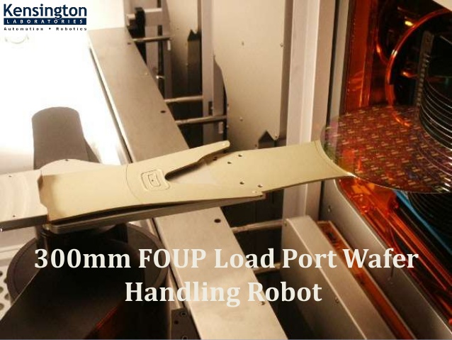
Semiconductor fabrication needs extreme accuracy. Wafer automation is essential because it replaces the delicate and repetitive duties of wafer handling and testing. Here's why it matters:
Accuracy and Consistency:
Automated systems guarantee that each wafer is handled and tested similarly, reducing human error and variability.
Increased Speed:
Automation substantially speeds up the mapping process, allowing for more throughput than human approaches.
Reduced Contamination:
Robots limit human interaction with wafers, lowering the risk of contamination from dust or particles.
Efficient Labor Use:
Wafer automation relieves professional technicians of repetitive chores, letting them to focus on process optimization and data analysis.
In the competitive semiconductor business, wafer automation is critical to enhancing efficiency, yield, and, eventually, delivering higher quality devices at a cheaper cost.
Benefits Beyond Quality Control
While ensuring quality is its primary role, wafer cassette mapping delivers broader benefits to the semiconductor industry:
Process Feedback:
Defect patterns on the map can point to weaknesses in specific manufacturing steps, allowing for targeted improvements.
Predictive Analytics:
Over time, wafer mapping data can form the basis of predictive models that forecast yield and identify potential issues early.
Smart Binning:
Mapping tools facilitate the classification of dies after the wafers are cut. For instance, faster dies can be reserved for high-end devices.
The Future of Wafer Cassette Mapping
As semiconductor technology pushes towards smaller, ever more intricate chips, the demands on wafer cassette mapping will only intensify. Expect to see advancements in accuracy and resolution to keep pace with shrinking feature sizes. Artificial intelligence (AI) will likely play a significant role in mapping systems, enabling more sophisticated pattern recognition for defects and deeper insights into process optimization.
Wafer automation will become increasingly sophisticated, further minimizing human interaction and potential errors. The integration of wafer cassette mapping with other stages of the manufacturing process will become tighter. Real-time data from mapping could potentially be fed into upstream manufacturing tools, allowing for immediate adjustments to improve quality and yield.
Wafer cassette mapping is already indispensable in the semiconductor industry. Its role will only become more critical as we enter an era of even greater chip complexity, ensuring the quality and performance of the electronics that power our world.


Comments
Post a Comment