Application of Silicon Wafers in Electronic Devices
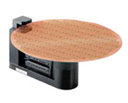
Silicon wafer is the main element in integrated circuits and is used in one-step production for moving firm substrates. Generally, the integrated circuit is a mixture of different electronic parts put together with silicon wafers placed on the main platform of semiconductor apparatuses. The wafer is finely cut for the semiconductor material so that it functions as the substrate over the wafer with microelectronic apparatuses incorporated.
The silicon wafer stage used in cohesive circuits is used in contemporary society daily. Computers, smartphones, and other gadgets are completely reliant on these apparatuses. Semiconductors are examined many times before they are incorporated into the devices. Silicon wafers are used in sensors to gauge tire pressure and solar cells. The wafer’s primary function is soaking up the photons in sunlight to generate electricity.

The silicon wafer stage used in cohesive circuits is used in contemporary society daily. Computers, smartphones, and other gadgets are completely reliant on these apparatuses. Semiconductors are examined many times before they are incorporated into the devices. Silicon wafers are used in sensors to gauge tire pressure and solar cells. The wafer’s primary function is soaking up the photons in sunlight to generate electricity.
Researches on Silicon Wafers
The silicon is used for producing superior silicon and other firm substrates for high-value applications. It gained attention because of its stupendous electronic, optical, and mechanical properties through conductive films. There were numerous challenges faced by films, to produce the films with minimum flaws to be used explicitly by semiconductors industries.
The wafers are made, keeping in mind the function of semiconductors on silicon, quartz, and other unbending substrates for completing the pending applications. Graphene film on a silicon wafer has numerous optoelectronic applications in the proof-of-concept stage. The transfer approach assists the market and has many benefits for bendable devices, which cannot be overlooked.
There is graphene on a copper-catalyst layer as well for covering a silicon substrate and acts as a great substitute. After production, the graphene is kept in position while the copper is scraped away. The graphene on the surface of the silicon wafer stage stops the delamination while scraping the copper catalyst, and after it, the graphene sticks onto the layer of silicon. A pre-treatment step is a vital step for entailing the insertion of gases into the wafer. It also modifies the interface properties for the development of permeation liquid used to remove the catalyst. During the co-addiction, the surfactants iron out any folds and creases generated in the transfer process.
Silicon wafers and other inflexible substrates are beneficial for the growth at load port appearing for the platforms, with an array of applications. Moreover, the interface transfer approach is preferred as it is responsive in batch-processing semiconductor manufacturing created for large-scale circuits on silicon wafers.


Comments
Post a Comment