Future of Semiconductor Manufacturing: How Wafer Handling Automation is Revolutionizing Production
The semiconductor industry is the backbone of modern technology, powering everything from smartphones and laptops to advanced medical devices and autonomous vehicles. As the demand for smaller, faster, and more powerful chips continues to soar, the industry is constantly seeking ways to enhance efficiency, precision, and throughput in manufacturing. One technology that's playing a pivotal role in this evolution is wafer handling automation.
Understanding Wafer Handling Automation
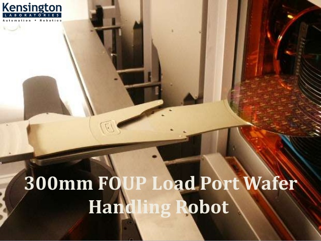
At its core, wafer handling automation involves the use of robotic systems and sophisticated software to manage the movement, processing, and tracking of semiconductor wafers throughout the manufacturing process. Wafers, thin slices of semiconductor material, are the building blocks of integrated circuits (chips). Traditionally, wafer handling was a labor-intensive and error-prone process, but automation has revolutionized it.
Benefits of Wafer Handling Automation
Wafer handling automation brings a multitude of benefits to semiconductor manufacturing, revolutionizing efficiency and quality:
Enhanced Precision and Consistency:
Wafers may be handled by automated systems with unmatched precision and repeatability, reducing the possibility of errors and guaranteeing a larger output of viable chips. This is important in an area where minuscule flaws may completely destroy a chip.
Increased Throughput and Efficiency:
Compared to manual handling, wafer processing can be done much more quickly thanks to robots' ability to operate nonstop, around the clock. Shorter manufacturing cycles and a quicker time to market for new semiconductor devices result from this.
Reduced Contamination Risk:
Because automated systems work in cleanroom settings, there is less chance of contamination from humans. Because wafers are so sensitive to impurities, even little particles can cause them to stop working properly.
Improved Traceability and Data Collection:
From manufacture to testing and packing, automation allows for the thorough tracking of every wafer. For yield enhancement, process optimization, and quality control, this data is priceless.
Cost Savings:
Wafer handling automation might have a significant upfront cost, but in the long run, the advantages outweigh the drawbacks. Manufacturers save a lot of money because they have lower labor costs, less error-related waste, and more efficient manufacturing.
Wafer Cassette Mapping:
Wafer cassette mapping is a crucial part of automating wafer handling. This entails utilizing machine vision or barcode scanning to accurately locate each wafer within a cassette—a container used to carry wafers. In a complicated production process, errors in wafer processing order might be fatal. Accurate cassette mapping guards against this.
Applications Across the Semiconductor Manufacturing Process
Wafer-handling automation is used at several phases of semiconductor production:
Front-End (FEOL):
Wafer production entails depositing small layers of material, etching complicated patterns, and doping the semiconductor with impurities. Robots play an important role in transferring wafers between processing machines and guaranteeing accurate alignment throughout these vital processes.
Back-End (BEOL):
Following fabrication, wafers are cut into individual chips, tested, and packed. Automated systems manage chip sorting, testing, and packaging activities, which improves total process efficiency.
The Future of Wafer Handling Automation
Wafer-handling automation will advance further as the semiconductor industry pushes technological boundaries. Observe the following trends:
- Artificial intelligence (AI) algorithms will be utilized more frequently to forecast equipment failures, improve system performance, and optimize wafer handling procedures.
- Robots will get more skilled and able to handle thin wafers with even more accuracy. It is also possible to use collaborative robots, or cobots, to operate alongside human operators, increasing their agility and flexibility.
- Automation of wafer handling will be easily incorporated into "smart factories," where networked devices interact and cooperate in real-time to maximize output.
Conclusion
In the semiconductor business, automation of wafer handling is revolutionary. It is more than just a technical development; for firms trying to stay competitive in a market that is changing quickly, it is a strategic need. There is no denying the advantages of automation: higher throughput, decreased contamination, enhanced accuracy, and cost savings.
Wafer handling automation will become more and more important as the demand for semiconductors rises, helping the industry to satisfy this need while upholding the highest standards of efficiency and quality. Wafer-handling automation is a technology that will continue to advance and become more widely used in semiconductor production.
.jpg)


Comments
Post a Comment