Find the Defects on a Wafer with Advanced Semiconductor Wafer Defect Inspection System
The semiconductor sector is mainly engaging in designing as well as fabrication of semiconductors. It has been analyzed that the automation sector is in great demand for the entire electronics manufacturing industry. There are many professionals who provide the best wafer stage solutions. So, you must rely on the best experts that will meet your exact demands.
When it comes to precision linear & rotary positioning stages, the semiconductor wafer inspection sector needs high precision. Metrology as well as inspection are considered the two essential terms used for the management of the semiconductor manufacturing process.
There are approx. hundreds of steps involved in the overall manufacturing process of semiconductor wafers which, of course, takes a lot of time. If any defects occur early in the manufacturing process, all the work undertaken to perform the steps will be wasted. That is why metrology & inspection processes must be established at critical points of the semiconductor manufacturing process. It ensures that a specific yield can be confirmed & maintained.
A high-speed wafer defect inspection system helps detect all the physical defects and pattern defects present on wafers & obtains the position coordinates (X, Y). Moreover, the defects can be divided into random defects as well as systematic defects.
Let us Now Discuss the Patterned Wafer Inspection System
There are several types of patterned wafer inspection systems, such as electron beam, brightfield, or darkfield inspection systems. Each of these inspection systems has its own features, but the basic detection principles are generally the same.
In the semiconductor wafer, the electronic devices of the same pattern are made alongside. There is a great possibility that random defects are usually caused by particles like dust & occur in random positions. However, the likelihood that they will repeatedly occur in a particular position is extremely low. However, the Patterned wafer inspection systems can detect defects by simply comparing the pattern images of adjacent chips & obtaining the difference.
In case many defects occur on the surface of a wafer, the circuit patterns are not created rightly, thus it causing the patterns to be missing. If there are several defects, they prevent the electronic circuit from operating accurately, thereby building the wafer as a defective product. Thus, detecting defects & specifying their locations are the major role of a wafer inspection system.
About Kensington Labs
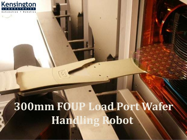
With Kensington as the wafer handling robot and precision motion control partner, you will get highly robust & reliable product lines which include wafer handling robot solutions and precision motion control solutions. We offer products that will meet the customers' specific needs for wafer handling robots and precision motion control applications. We have a perfect team of professionals who work with full dedication & passion to fulfil the exact demands of the customers. Kensington possesses a long history of delivering robust precision automation solutions. If you need precision motion control solutions, get in touch with us today!


Comments
Post a Comment