Essential Role of Front-End Processes in Semiconductor Manufacturing
The front-end processes play a crucial part in creating the silicon chips that power our contemporary gadgets in the complex world of semiconductor production. The purpose of this blog article is to provide insight into the importance of wafer front-end procedures and the crucial processes that turn silicon raw into the intricate integrated circuits (ICs) seen in commonplace gadgets.
Understanding the Semiconductor Front End
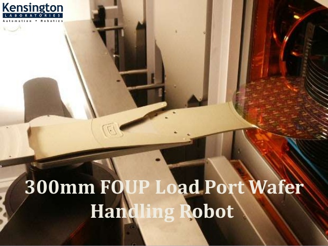
The semiconductor front end, commonly referred to as wafer front end or wafer fabrication, refers to the early phases of semiconductor manufacture. Transistors, diodes, and other basic components are made on a silicon wafer using these procedures. The integrated circuit is built on the wafer, and the intricate circuitry that follows is made possible by the front-end operations.
Key Processes in Wafer Front-End Manufacturing
The wafer front end of semiconductor production involves a complex and intricate set of procedures. These processes are not just about converting a raw silicon wafer into integrated circuits (ICs) for electronic devices. They are about laying the foundation for the electrical components and connections that will form on the wafer, a task of utmost importance.
Wafer Preparation: First, a silicon wafer has to be made. This is usually done by slicing a cylindrical ingot of pure silicon. A flawless, smooth surface prepared for additional processing is ensured by cleaning and polishing.
Oxidation: Through oxidation, a thin layer of silicon dioxide (SiO2) is generated on the surface of the wafer. This oxide layer is important for further masking and etching procedures because it acts as an insulator.
Photolithography: This crucial process is etching complex circuit designs into the wafer. Using a patterned mask, the light-sensitive photoresist is applied and subjected to UV light. The intended design remains on the wafer after the exposed photoresist is removed.
Etching: Etching uses the photolithography-defined pattern to selectively remove parts of the wafer material. As a result, transistors and other components' physical structures are created. Techniques for both wet and dry etching are used to remove material precisely.
Deposition: The wafer surface is covered in thin layers of different materials. Depending on the particular part being made, these films may be semiconductors, insulators, or conductors. Common deposition techniques include chemical vapor deposition (CVD) and physical vapor deposition (PVD).
Doping: Impurities are added to change a semiconductor material's electrical characteristics. The kinds and concentrations of impurities present determine the conductivity and behavior of the components generated on the wafer.
Metallization: To build the connections between different components on the wafer, metal layers are deposited and patterned. The complex wire network made up of these metal lines allows electrical impulses to go throughout the integrated circuit.
The wafer front end establishes the basis of the semiconductor chip. The accuracy and caliber of these operations directly impact the finished semiconductor devices' yield, performance, and dependability. Thanks to developments in wafer front-end technology, integrated circuits are becoming increasingly miniaturized.
Importance of Semiconductor Front End
The core of the whole semiconductor manufacturing process is the semiconductor front end, sometimes referred to as the wafer front end. Raw silicon wafers go through crucial changes in this first phase, laying the groundwork for the complex integrated circuits (ICs) that drive our digital world.
Quality & Performance: Front-end operations like photolithography, etching, and deposition have a direct impact on the yield, performance, and dependability of the final semiconductor devices.
Innovation Catalyst: The shrinking of transistors is fueled by advancements in wafer front-end technology, like as extreme ultraviolet (EUV) lithography, which makes processors smaller, quicker, and more energy-efficient possible.
Economic Impact: The front end of semiconductors is a high-stakes game. At this point, errors or inefficiencies might result in chips that don't work properly, reduced manufacturing yields, and eventually higher prices for both customers and producers.
The semiconductor front end is essentially the interface between precise engineering and invention. Acquiring proficiency in this phase is essential not just for manufacturing superior chips but also for propelling technological advancement and preserving a competitive advantage in the worldwide semiconductor sector.
Conclusion
Semiconductor front-end procedures are critical in the development of integrated circuits that drive today's technology. From wafer preparation to metallization, each step at the front end is critical in molding the silicon chips that power our cellphones, laptops, automobiles, and a variety of other gadgets.
As technology advances, the need of mastering and improving wafer front-end processes will only increase, ensuring that we continue to benefit from increasingly complex and powerful semiconductor devices.


Comments
Post a Comment