Wafer Handling Robot and EFEM: Enhancing Semiconductor Performance
A wafer-handling robot is a robotics system that automates the handling of silicon wafers during the manufacturing process of semiconductors. Several tasks are executed by the wafer-handling robots, such as cassette mapping, wafer distribution, and wafer tilt check. These are highly beneficial in lessening adulteration during wafer processing. Nevertheless, they demand a high initial acquisition.
Applications of wafer-handling robots
In unified circuit manufacturing, a wafer-handling robot moves and adjusts wafers. These facilitate the rate of product flaws by pushing products quickly and in a way that is correct in all details.
These are very common in the industrial sector and can be used to:
- Move materials from one workstation to another.
- Select, style, package, and palletize products.
- Push parts and elements from one assembly line to another.
- Deliver a part to a welding robot.
- Transmit a member to a conveyor belt.
- Maintain a piece in place for production.
The robots can also motorize various reductant tasks in manufacturing or machine tool shops. For illustration, a machine-trending robot can position workpieces within machine tools and withdraw them once an operation is finalized. This post will shed light on how wafer-handling robots and EFEM improve semiconductor manufacturing.
Intent
There is no denying that nowadays, electronic industries rely tremendously on robotics for production. To move wafers between wafer processing levels, a wafer-handling robot is utilized. Generally, a pick-measure-place procedure is employed for transferring wafers with accuracy. To boost the wafer transfer effectiveness, optic detectors are installed at each station to assess the wafer's peculiarity on the fly. The eccentricity values are then applied to correctly manage the robotic placement of the wafer directly onto another station.
Design
The kinematics model of the wafer-handling robot is designed to enhance semiconductor manufacturing. Two detector spot calibration algorithms are proposed. Method I is about the wafer-handling path, and Method II utilizes the offset approaches from the wafer-handling path. Then, the outcomes of both methods are analogized. To compute the wafer eccentricity on the fly, a wafer eccentricity estimation technique is produced.
Determinations
The designed methods are then executed with a wafer-handling robot in the semiconductor manufacturing process. The wafer idiosyncrasy assessment errors are significantly reduced with the help of the formed methods. Furthermore, it has been found via experimental outcomes that Method II achieves more favorable results and thus can be utilized for improving the wafer handling robot's accuracy and efficiency.
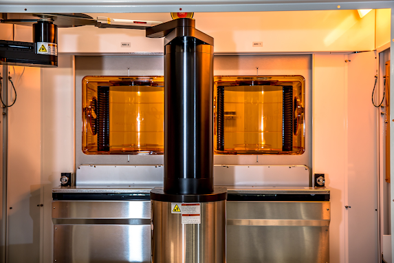
Equipment Front End Module or simply an EFEM is a wafer-loading module that drives products between storage carriers, processing dimensions, and testing systems. These are the central components of semiconductor automation.

An EFEM control software controls an assortment of one or more Buffer modules, Aligners, Robots, Load Ports, etc. Furthermore, the software that operates on the EFEM handles all possible varieties of devices without having to make amendments to the software.
Conclusion
Both EFEM and wafer-handling robots ensure the successful manufacturing of semiconductors. In the post as mentioned above, we have explained detailed information about the wafer handling robots.


Comments
Post a Comment