Maximizing Yield in 300mm Semiconductor Front End Processes: Critical Role of FOUPs
In the complex world of semiconductor production, where yield optimization at the front-end processes is critical and efficiency is the ultimate goal, the 300mm FOUP (Front Opening Unified Pod) has become a key component. This humble carrier is essential to protecting the fragile wafers that are the foundation of contemporary technology.
Understanding 300mm FOUPs
A 300mm FOUP is essentially a customized container made to move and hold silicon wafers throughout different phases of the production of semiconductor front end. Dust, moisture, and even minute concentrations of chemicals can cause these wafers to become very susceptible to environmental pollutants. The main purpose of the FOUP is to protect these wafers from any damage by offering a hermetically sealed, ultra-clean environment.
Importance of Yield in Front-End Processes
Yield, the percentage of functioning chips generated from a wafer, is an important measure that influences profitability and efficiency. Even minute impurities or handling mistakes in sensitive techniques such as lithography, etching, and deposition can result in catastrophic yield reductions.
This is where the 300mm FOUPs (Front Opening Unified Pods) come in. These unique carriers create a hermetically sealed, ultra-clean environment that protects wafers from contamination and physical harm. FOUPs are critical to maximizing yield throughout the semiconductor front end process because they reduce the likelihood of faults during transport and storage.
Essentially, FOUPs are the unsung heroes that ensure the successful transformation of raw silicon wafers into the high-performance chips powering our modern world. Their contribution to yield optimization is not just a technical necessity; it's a financial imperative for the semiconductor industry.
FOUPs as Yield Guardians
In the high-stakes world of semiconductor front-end manufacturing, where a single speck of dust can ruin a chip, 300mm Front Opening Unified Pods (FOUPs) stand as unsung heroes, safeguarding yield at every step.
Contamination Control:
FOUPs' hermetically sealed construction produces a perfect microenvironment that protects sensitive wafers from chemicals, moisture, and airborne particles that can severely affect yield.
Automated Handling:
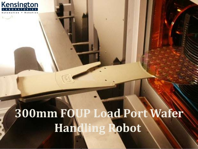
FOUPs seamlessly integrate with automated material handling systems (AMHS), minimizing human intervention and the risk of contamination or damage during wafer transport. This streamlined process enhances efficiency and protects product integrity.
Wafer Protection:
The FOUPs' robust construction acts as armor for wafers, safeguarding them from physical shocks and vibrations during transit. This is crucial, as even minor damage can compromise a wafer's functionality.
Traceability:
Due to the unique identifiers attached to each FOUP, careful tracking is possible throughout the production process. Continuous improvement may be achieved by locating and isolating any sources of contamination or yield loss thanks to this traceability.
FOUPs are more than simply carriers; they are the keepers of yield, making sure that every 300mm wafer is used to its maximum potential and helping to produce the high-grade semiconductor chips that run the contemporary world.
Innovations in FOUP Technology
FOUP technology has advanced because of the constant search for increased yields and more productive manufacturing techniques. Some notable innovations include:
- Advanced Sealing Mechanisms: More recent FOUP designs have better sealing mechanisms that uphold even higher standards of cleanliness inside the pod.
- Smart FOUPs: These FOUPs have sensors that keep an eye on things like humidity, temperature, and particle count. The proactive management of contamination is made possible by this real-time data.
- Mini-Environments: In order to better improve wafer processing, certain FOUPs are made to generate a mini-environment with certain atmospheric conditions, including low humidity or particular gas combinations.
The Future of 300mm FOUPs
With the semiconductor industry always striving to reduce size and increase intricacy, 300mm FOUPs will probably play an even more crucial role. Wafer protection and strict contamination control will become more and more important with the introduction of cutting-edge technologies like extreme ultraviolet (EUV) lithography and 3D stacking.
In conclusion, the 300mm FOUP is a protector of yield in the semiconductor front-end rather than just a carrier. Its significance in automation and traceability, together with its capacity to protect fragile wafers from damage, make it an essential instrument in the pursuit of dependable and efficient chip fabrication. The modest FOUP will continue to change as technology develops and will be crucial in determining how the semiconductor industry develops in the future.


Comments
Post a Comment