From Wafer to Chip: Exploring Semiconductor Front End Advancements
Every advanced technology relies on semiconductors for their operation as the modern world functions through them. These miniature components are the foundation for all modern advanced technologies, whether smartphone processors or high-performance computers. Have you ever wondered what it takes for a wafer to become a functioning electronic chip?
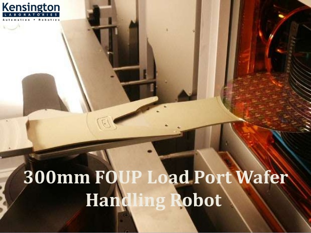
Front-end operations of the semiconductor begin at this vital process stage. Wafer fabrication and precise processing methods at this phase form the basis for high-quality semiconductor devices. The evolution of technology has led to more precise wafer handling methods that Semiconductor Robot Handling implements. Semiconductor front end technology brings the latest advancements as automation transforms chip manufacturing operations.
Understanding the Semiconductor Front End Process
The Semiconductor Front End comprises the first semiconductor manufacturing half, through which silicon wafers undergo elaborate manufacturing steps to develop microchip base structures. These steps include:
- Wafer Cleaning: Eliminating contaminants from the wafer surface constitutes one of the most critical aspects of semiconductor processing.
- Photolithography: The process involves the transfer of circuit patterns to the wafer.
- Etching: Removing unwanted material to define chip structures.
- Deposition: Adding thin layers of materials for conductivity and insulation.
- Doping: The addition of specific impurity types enhances the semiconductor's electrical characteristics.
Each procedure needs to be executed with exact precision standards. The slightest imprecision creates defects that decrease production and raise manufacturing expenses. This is where Semiconductor Robot Handling becomes a game-changer.
How Semiconductor Robot Handling is Transforming the Industry
Gone are the days when semiconductor wafers were handled manually or with limited automation. Today, Semiconductor Robot Handling systems ensure:
- Higher Precision: Robots eliminate human errors, ensuring accurate wafer movement.
- Increased Efficiency: Automated systems function without human intervention across all 24 hours, which helps decrease production duration.
- Better Yield: The elimination of contaminants and defective handling operations produces superior chips.
- Safer Work Environments: Reducing human interaction with hazardous materials.
Advanced wafer-handling robots feature sub-micron precision and operate effectively in ultra-clean manufacturing spaces to become vital components of the semiconductor production chain.
The Future of Semiconductor Front-End Technology
The growing need for quicker, smaller, and more cost-effective microchips pushes semiconductor manufacturers to stay ahead with modern technology. These newest innovations consist of:
- AI and Machine Learning in Wafer Inspection: The ability to detect defects during real-time operation supports improved production quality.
- Extreme Ultraviolet (EUV) Lithography: These advancements make the manufacture of tiny transistors needed for next-generation chip development possible.
- Fully Automated Smart Factories: The combination of robotics technology with data analytical systems creates a perfect manufacturing system.
The future development of Semiconductor Front-End processing depends heavily on robotics and automation, which will boost efficiency while enhancing reliability standards.
Conclusion
The adventure from wafer to chip is a wonder of engineering and innovation. With improvements in Semiconductor Front End technology and Semiconductor robot handling, producers are achieving new levels of efficiency and precision in chip manufacturing.
Kensington Labs is committed to imparting the most dependable and innovative wafer-handling robots and precision motion control stages, guaranteeing semiconductor producers meet the ever-developing requirements for high-performance chips.
As the semiconductor enterprise continues to develop, one thing is clear—automation and robotics are paving the way for the next generation of microelectronics.


Comments
Post a Comment