Essential Tips for Choosing the Best Wafer Fabrication Equipment for your Application
The semiconductor industry lies at the core of technological advancement as a species. Driverless cars, highly advanced mobile phones, and IoT networks all rely on chipmakers who can fulfill the increasingly formidable quality as well as quantity needs. But to answer this demand, the semiconductor manufacturers require the appropriate approach, the right technologies, as well as an unshakable eye for the details.
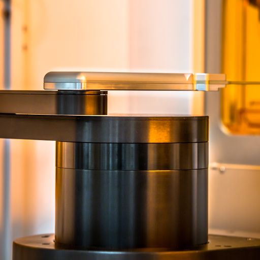
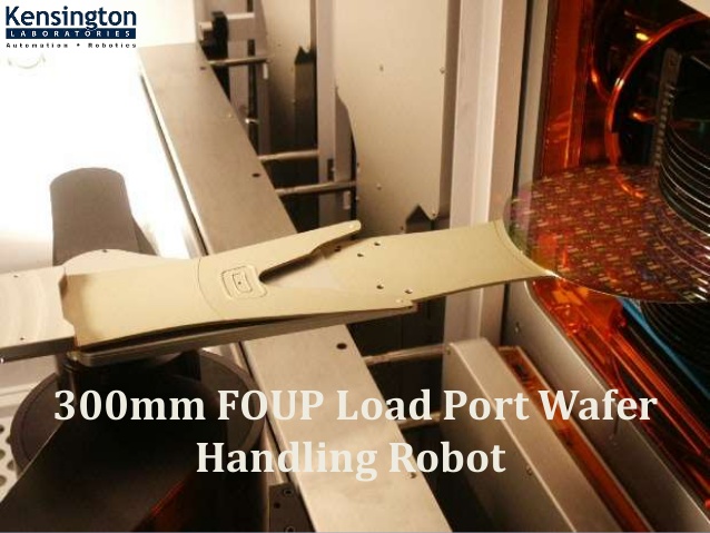
When it comes to wafer handling in the EFEM module, like the end effector or the pre-aligner, Kensington labs give you high precision. In this blog, you can see essential tips for semiconductor manufacturers who want to maintain their relevance & enhance their yield.
Check out the Special Tips for Semiconductor Fabrication
Do not Underestimate the Importance of Cleanliness
There are some manufacturing environments in which cleanliness is of great importance. We are here talking about products with tolerances measurable down up to the millionth of a centimeter. In semiconductor manufacturing, even a single dot of dust can set you back, so it is always worthwhile to reconsider the equipment & protocols you use to keep your facility clean — & to double down on maintenance as well as regular cleaning. In addition, one must be highly careful while handling the semiconductor front end and back end processes.
One Should Know All the Relevant Industry Standards
With the continuous growth of the semiconductor industry, there is no surprise that standards in this field see regular revisions. SEMI E176-1017 standard is among the more recent semiconductor standards & one that every company would do well to keep top of mind as they scale their operations to fulfil the exact demand. Basically, this all-new standard describes a holistic approach to addressing electromagnetic interference in the fabrication environment.
Automate Where You Can Enhance Throughput
In the world of semiconductors, all the semiconductor manufacturers could prioritize throughput as well as processing time equally to enhance the productivity of their operations. Thanks to the expanding accessibility of automation technology, you may find that the throughput is one of the lower-hanging fruits to pick. Semiconductor fabrication facilities increasingly leverage robotics as well as other automated tools in order to handle wafers & other materials and to cut down on lossy & potentially error-prone manual transportation, error detection as well as calibration between processes.
Select the Right Equipment & Provider
As productivity & livelihood depend on your mechanical assets, it is important to work with a company which stands behind their equipment, designs for safety, & makes it simple to schedule on-site repairs as well as maintenance when something goes wrong. So, it is always convenient to choose the right equipment provider.
Leverage the Smarter & Advanced Technologies
Finally, we land one of the best points to consider in semiconductor manufacturing. It basically describes an ‘integrated intelligence’ in fabrication equipment that monitors the temperature, position, voltage, speed, angle, position & manifold other variables that would be difficult to measure in real-time by any other means. Thanks to automotive technology as it is taking off, semiconductor manufacturers find themselves up to increasingly stringent quality standards.
When investing in companies, it's important to consider all the critical factors which are mentioned above. If you want to learn more regarding the wafer front, feel free to talk with experienced professionals.


Comments
Post a Comment