A Quick Guide to Semiconductor Wafer Front End Electronics Manufacturing
If you are an electronics engineer, you might have an idea about Semiconductor Front End manufacturing.
Semiconductor manufacturing is basically divided into two parts one is known as Front End Manufacturing, and the other is known as Back-End Manufacturing. semiconductor manufacturing is referred to as the fabrication process as all the features/circuits have been created on the wafer. A fusion of extreme accuracy and precision with high throughput makes for exciting technology.
Do you know that servo drives are used in several processes in backend semiconductor manufacturing because they offer fantastic performance & repeatability; This is what is precisely required in high-end semiconductor fabrication. Front end and backend processes involved in semiconductor manufacturing processes are particularly useful as they often augment & provide proper visualization to the backends of things that, sometimes, are not particularly visible parts of projects. Even I think being an electronics engineer, it would be quite difficult to perform front-end electronics manufacturing as it is one of the critical processes involved in semiconductor production.
Let’s Discuss Briefly Front end Electronics Manufacturing
The term ‘frontend’ electronics manufacturing is referred to as a part of the process of semiconductor manufacturing. Every semiconductor electronic, like MC(Microcontroller), logic ICs, & even simple MOSFET transistors, are produced via involving many processing steps before being delivered to the market.
Frontend manufacturing is known as the wafer fabrication & probing process, wherein backend manufacturing is the process where the wafer is cut, assembled, & packed into different packages. The semiconductors after that take the shape of the QFP, SOP, SOIC, and other common form factors used in the PCB design.
In most semiconductors factories, frontend electronics manufacturing starts by doping semiconductor wafers. It is a process that turns certain areas on the insulative silicon into conductive regions. Doping is generally performed by introducing doping gases on the silicon die in a furnace, referred to as diffusion.
The silicon dies can also go through the process of photo masking. The non-protected areas are eventually etched by using the solvent. The metal disposition also forms part of the frontend manufacturing process. After going through the whole process, the wafer’s thickness is then reduced in a process. Then the wafer probing starts validating the functionality of the die & fabrication process. Wafer dies that qualify for the probe test will be finally sent for backend manufacturing.
There are many challenges in front-end electronics manufacturing to deliver functional silicon wafers. Even a small mistake in the estimation during the manufacturing process may lead to unsatisfactory results.
Another challenge for front-end electronics manufacturing is the occurrence of static charges. In ESD, the charges could contaminate and damage the wafer during or after the front-end manufacturing process. It may reduce the yield of manufacturing. All thanks to the advancement of science and technology, which helps improve yield in frontend electronics manufacturing.
How to Improve Frontend Electronics Manufacturing?
Yield is the primary figure for manufacturers, & several strategies have been taken to enhance the efficiency of front-end manufacturing. The IoT in Industry 4.0, which leverages data, has enabled manufacturers to detect faults in the process line in a better way. With this technology, the manufacturers have better control of analytics & yield improvement.
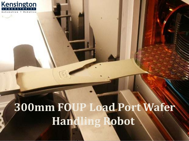
As the usage of machines has been increased, it thereby minimizes human interactions & the installation of better air circulation systems. It also reduced the contamination of the wafers. With the unique design and analysis tools available for Wafer Front End manufacturing from Kensington labs, you will get the high-end wafer handling robots.
Talk to us today if you’re looking for the best solutions!


Comments
Post a Comment