Why Multi-Axis Motion Matters in Semiconductor Wafer Handling
.jpg)
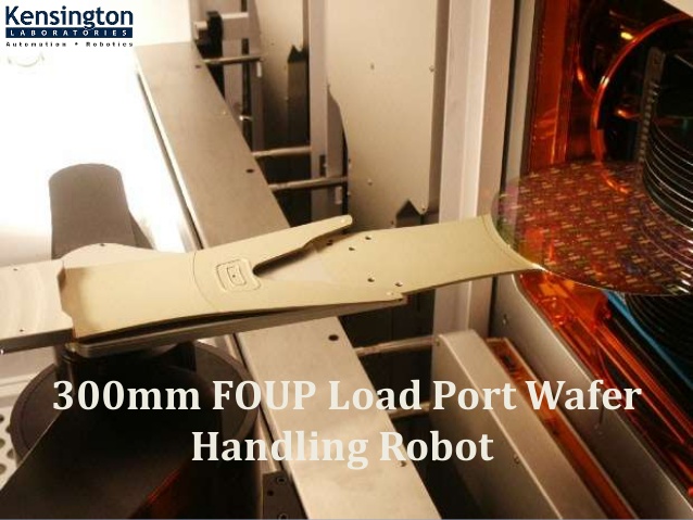
Modern chip manufacturing operates on sub-micron tolerances where even microscopic vibration can destroy an entire silicon batch. Moving fragile 300mm wafers between load ports, inspection stations, and process chambers requires far more than basic pick-and-place mechanics. It demands smooth, coordinated movement across multiple spatial directions simultaneously.
Engineers must balance extreme speed against mechanical stability. This is why multi-axis motion systems form the backbone of modern front-end semiconductor tool design.
The Complexity of Automated Wafer Transfer
Wafer movement might look straightforward on paper, but spatial constraints inside cleanroom environments complicate things. Transferring a wafer involves navigating restricted transfer slots, adjusting for rotational misalignment, and maintaining exact vertical positions during handoffs.
To meet these tight physical demands, wafer handling automation relies on dynamic coordinate control across several key axes-
Radial (R-Axis)- Manages linear extension and retraction into process chambers.
Rotational (Theta Axis)- Rotates the robot body to align with different tool ports.
Vertical (Z-Axis)- Controls precise lift and lower movements during wafer picks and places.
Wrist/Pitch Axis- Compensates for slight tilt or thermal expansion across long reaches.
Single-axis or rigidly uncoupled mechanisms lack the dexterity required for compact equipment layouts. By coordinating these individual axes in real time, modern platforms keep wafer trajectories flat, smooth, and predictable.
Architectural Advantages - Multi-Link Robots and Motion Control
System designers typically face a choice between standard SCARA configurations and articulated multi-link architectures. While SCARA units work well for simple pick-and-place tasks, high-density tool layouts require greater spatial flexibility.
Using multi-link robots gives tool builders a distinct advantage. These systems use multiple articulated joints working in tandem to navigate tight internal envelopes without swinging the robot arm out into structural frame boundaries.
Advanced robotic motion control algorithms calculate real-time kinematic transformations across all active joints. This eliminates harsh jerk forces during acceleration and deceleration.
Without coordinated acceleration profiles, rapid movements cause wafer slippage against the end effector - generating destructive ceramic or metallic particles inside cleanroom spaces. Integrated closed-loop feedback systems continuously correct path trajectories, protecting wafer surface integrity throughout the transfer cycle.
Key Benefits of Multi-Axis Motion Systems
Implementing flexible multi-axis motion systems directly impacts fab productivity, yield retention, and tool footprint.
.jpg)
1. Superior Yield Protection Through Precision Handling
Achieving precision wafer handling is impossible if mechanical vibration shifts a wafer even a fraction of a millimeter off-center. Multi-axis coordination allows the end effector to gently approach, lift, and retract from cassette slots with zero mechanical impact.
2. Space Optimization in Modern Semiconductor Robotics
Cleanroom floor space comes at a premium. Integrating multi-axis semiconductor robotics lets OEMs build tighter Equipment Front-End Modules (EFEMs). Robots can reach around internal structural pillars or serve dual-tier process chambers without increasing overall machine width.
3. Increased Throughput Across Complex Equipment
Every millisecond spent waiting for a robot arm to settle or realign adds up over thousands of daily wafer passes. High-speed multi-axis wafer transfer systems execute combined rotational and linear moves simultaneously, cutting total move times while maintaining exact spatial repeatability.
Evaluating Motion Architecture for Your Tool
Picking the right motion setup means looking at your robot as a connected system rather than a collection of separate parts. A great motor won't help much if the arm flexes under load or the controller can't keep up with path adjustments.
Key factors engineering teams evaluate include-
Payload and Arm Reach- Ensuring the robot comfortably supports a 300mm silicon wafer and heavy end effector without arm droop or deflection.
Repeatability Limits- Achieving sub-micron positioning accuracy over thousands of continuous transfer cycles.
Cleanroom Compliance- Meeting strict ISO Class 1 and SEMI standards to prevent outgassing and particle generation.
Controller Responsiveness— Handling real-time multi-axis interpolation to keep acceleration trajectories smooth.
Building a reliable transfer system comes down to balance. Structural stiffness, motor torque curves, optical encoder feedback, and vacuum grip controls must all be tuned together to keep wafer handoffs fast and safe.
Concluding Thoughts
Maximizing tool uptime and wafer throughput depends on how smoothly your automation handles delicate substrates. As node sizes continue to shrink, relying on rigid, low-axis transfer methods introduces unnecessary positioning errors and yield risk.
Upgrading to versatile multi-axis motion systems gives semiconductor tool manufacturers the spatial dexterity, trajectory control, and continuous repeatability needed for modern fab operations.
When evaluating high-precision automation components or refurbishing legacy tool platforms, working with experienced industry pioneers like Kensington Laboratories ensures your robotics deliver long-term reliability, seamless integration, and ultra-clean performance across every transfer cycle.


Comments
Post a Comment