Unveiling the Semiconductor Front End: The Crucial First Stage in Chip Manufacturing
The semiconductor industry, driving the digital age, is a powerhouse behind numerous technologies we rely on daily. Whether smartphones, computers, or vehicles, semiconductors form the core of modern electronics. The production of these chips is a complex, multi-stage process, with the Semiconductor Front End being the crucial first stage in chip manufacturing. This blog will delve into what the Semiconductor Front End entails, why it is essential, and how it lays the foundation for the advanced chips that power the modern world.
What is the Semiconductor Front End?
The Semiconductor Front End refers to the initial phase of semiconductor chip manufacturing, where the silicon wafer is prepared, and integrated circuits (ICs) are formed. This stage primarily takes place in a cleanroom environment due to the need for precise conditions that prevent contamination from dust, particles, and other contaminants. The goal of the front-end process is to create the active regions of the chip where electrical currents will flow and be controlled. It involves intricate steps like:
Wafer Fabrication – The process begins with the creation of a wafer, typically made of silicon. This wafer is the substrate upon which the integrated circuit will be built. Once sliced from a silicon ingot, the wafer undergoes rigorous cleaning and polishing.
Photolithography – A vital part of the front end, photolithography involves using light to transfer geometric patterns onto the silicon wafer's surface. A photoresist is applied to the wafer, which is then exposed to ultraviolet light through a mask with the desired pattern. This is followed by developing the wafer to create the circuit pattern on its surface.
Etching – After photolithography, etching removes material from the wafer's surface to form the chip's intricate designs. Etching can be done through wet or dry methods, using chemicals or plasma to carve out the patterns left by photolithography.
Doping – To control the flow of electrical currents, certain areas of the wafer are doped with impurities such as boron or phosphorus. This process is critical in defining the electrical characteristics of the transistors and diodes that will form the basis of the chip.
Thin Film Deposition – Thin layers of materials like oxides or metals are deposited on the wafer to create insulating layers and interconnect. This process forms the backbone of the circuits and ensures that signals travel efficiently across the chip.
Why the Front End is Critical
The Semiconductor Front End is critical because it sets the stage for the entire manufacturing process. Any mistake in this early phase, whether during photolithography or doping, can lead to defective chips that fail to function properly. The precision required in each step is immense, as chips are becoming smaller, more complex, and more efficient over time.
As semiconductor technology advances, the demand for smaller and more powerful chips grows, making front-end processes even more vital. Front-end innovation is driving the production of next-generation chips that power artificial intelligence, 5G networks, and Internet of Things (IoT) devices.
Challenges in the Front-End Process
Manufacturing semiconductor chips is incredibly challenging, especially as chip features shrink to nanometer scales. Achieving high yields of functional chips requires minimizing defects, maintaining ultra-clean environments, and constantly innovating photolithography techniques to create ever-smaller circuits.
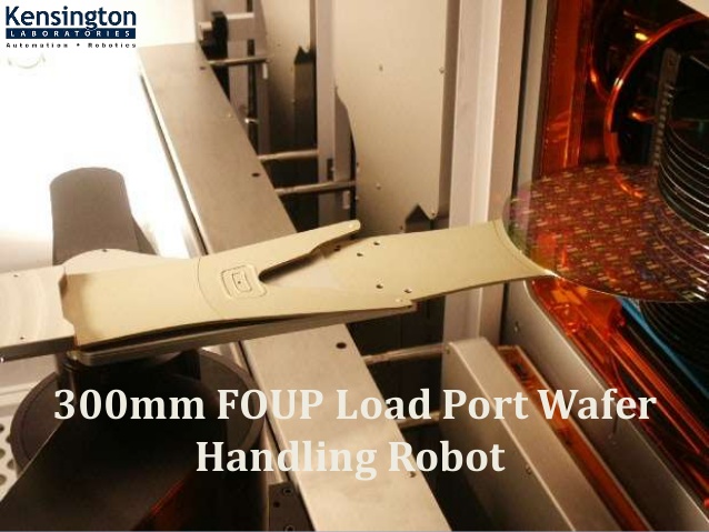
In the front-end process, wafer handling is crucial as it impacts the yield and overall success of the chip production. Precision handling of wafers, particularly as their dimensions decrease, becomes more difficult but critical to avoiding contamination and damage.
Conclusion
As chip designs continue to evolve and shrink, the demands on the Semiconductor Front End process will only grow. Companies involved in automation and robotics are key players in supporting this evolution. Kensington Labs is committed to providing the most reliable and innovative wafer handling robots and precision motion control stages, ensuring that the complex front-end processes run smoothly and efficiently.
In an industry where precision is paramount, Kensington Labs' solutions empower semiconductor manufacturers to stay ahead of the curve, delivering high-quality chips that are the foundation of our digital future. With continued advancements in automation, the semiconductor industry will push the boundaries of what’s possible, all starting with the critical Semiconductor Front End process.


Comments
Post a Comment