Chips & Wafers: Basic Building Blocks of Semiconductor Industry
After manufacturing and processing, an integrated circuit's layout and area consideration is crucial to maintaining the form factor. The wafer manufacturer specifies design rules, which the design engineer must follow when laying out the integrated circuit. Minimum clearance values are typically required between diffused regions, contact windows, and metalized contacts to account for mask registration issues and minimal line resolution.
What is a Wafer?
For the production of semiconductor devices, a wafer is a thin slice of material, often spherical and with a mirror-like finish surface. Crystal growth, wafer forming, wafer polishing, and wafer preparation are the four main categories that categorize wafer manufacturing, both wafer front end and wafer back-end manufacturing. The final product of the first wafer fabrication stage is a crystal ingot with a particular crystalline property. The sliced wafer is created during wafer shaping with specific dimensions and thicknesses. Wafer polishing is carried out to prepare the wafer surface for producing semiconductors, and then the finished product, a package of prime wafers, is prepared. Metallurgical grade silicon, produced by carbon-thermic reduction of silica in an electric arc furnace, is the raw silicon needed for semiconductor devices. This unprocessed silicon is transformed into a crystal substrate that needs additional purification.
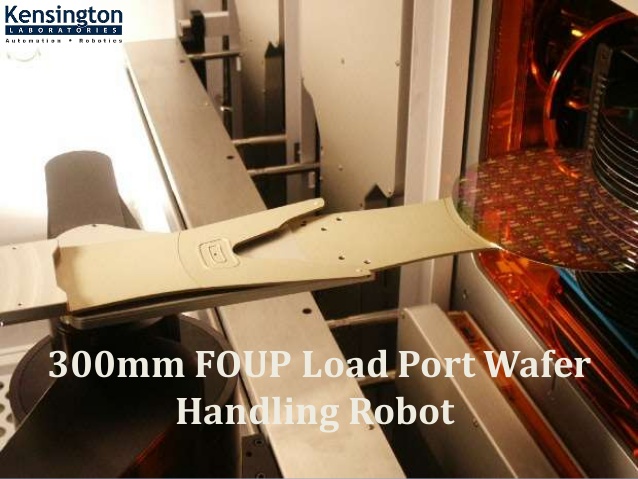
Due to its significance in manufacturing electronic components assembly, wafer thinning has recently attracted a lot of attention. The diameter of silicon wafers varies from 300mm to 25.4mm, depending on the application.
However, the fabrication labs employ 300mm technology and gradually increase in diameter to embrace 450mm in order to lower costs and increase throughput.
High-performance radio frequency applications that use silicon from the sapphire process often use silicon wafers. Good linearity, good isolation, and a high tolerance for electrostatic discharge are just a few of Sapphire's insulating advantages. Optical devices can also be made with silicon on sapphire. Because a 12-inch wafer is difficult to slice, silicon wafers are challenging to make. Using a diamond disc, the edge is smoothed, and any damage is removed. Despite the difficulty in producing silicon wafers, silicon is still one of the most widely utilized elements in electronic devices because of its abundance.


Comments
Post a Comment