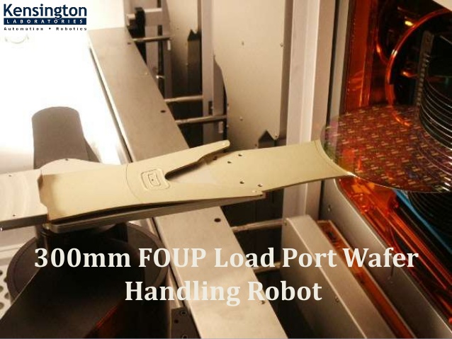
Semiconductors are a powerful technology with advanced innovation, from the first autonomous vehicle to the first space flight. They are extensively utilized in various goods we rely on daily, including computers, smartphones, and other transportation and manufacturing equipment. Every part of our lives has been improved by advancements in semiconductor technology, making it easier, safer, and more efficient. Due to the rise in demand for semiconductor manufacturing, numerous semiconductor handling equipment also increased. This is where Kensington Laboratories comes into the picture with its products, such as wafer-handling robots, Kensington controller, wafer pre-aligners, etc.
The cost of innovation is increasing for semiconductor manufacturing and design, so the semiconductor business is not an exception and continues to confront both internal and external challenges. Innovation costs rise externally as investment costs rise gradually while manufacturing stays an internal delicate and intricate process requiring a highly controlled environment.
Continuously Evolving Needs
Manufacturers and R&D facilities require sensitive and reliable analytical testing solutions because they are constantly trying to better processes. Equipment that can detect critical impurities at low levels and combine seamlessly with online sampling accessories is needed to increase productivity and uptime.
Increased Demand
With rising demands, trends like automation, electrification, digital connectedness, and security compelled the industry to develop and use more sophisticated or modified silicon-type wafers. Due to their superior thermal properties, silicon carbide wafers are used in optoelectronics, solar converters, and industrial motor drives. Additionally, semiconductors open up new demand sources by enabling the development of emerging markets for things like artificial intelligence (AI), quantum processing, and advanced wireless networks.
If you are looking for the best M4000 controller, look no further than Kensington Laboratories.
Defect & Failure Identification
Testing at various stages is required, commencing with the raw materials at the outset of the process, as wafer defect management issues can arise at any point during the manufacturing process. Various analytical methods can be used to determine the materials' elemental and organic composition and physical testing. A functional surface on a wafer will combine the characteristics of the substrate and the functionalized group to create a material that can combine elements of each after the starting materials are added to the manufacturing process. The wafers may also receive coatings to help with wafer processing or to provide the features needed for additional processing. Any remaining contaminants can harm the performance of the wafer and the finished product. Therefore, impurity detection and management are crucial during the entire manufacturing process.
Examining Obstacles
Scale is the most significant challenge in semiconductor wafer testing since devices are continuously getting smaller, necessitating tools with better precision detection. The industry may need to move to alternative materials to grow and meet the rising demand for devices, which necessitates the growth of entirely new procedures and more analytical practices.
Semiconductor manufacturing is the need of the hour. And we have to look for numerous ways to expedite the production of semiconductors.


Comments
Post a Comment