Solving the Obstructions in Semiconductor Front End Manufacturing!
Chip manufacturers Intel and Samsung Electronics are the most important businesses in this sector. Semiconductors are essential to many regularly used electronic products, including smartphones, tablets, IoT devices, and PCs. Semiconductor front-end manufacturing, which represents the first set of steps in a semiconductor fabrication workflow, is one of many forms of manufacturing.
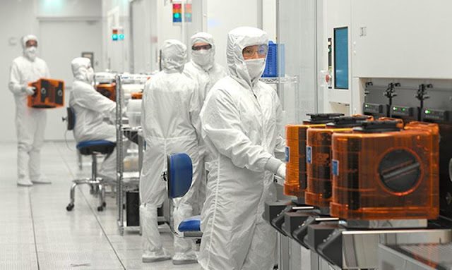
Extreme accuracy and precision are required. They typically come after crystal growth and wafer extraction and before what is known as the "back-end procedures" that include IC assembly. A series of partners with expertise in one or more semiconductor manufacturing processes typically manage this complex manufacturing chain, partly because the semiconductor industry was so vulnerable to supply chain issues brought on by the pandemic.
Customers in the next-generation semiconductor industry need smaller sizes and geometries, which is where polymer sealing solutions can be helpful in the increasingly demanding and difficult manufacturing processes seen in the current environment. Polymer materials can withstand stronger chemicals and higher temperatures, which add to the equipment's wear and tear. This increases the equipment's lifespan, lowers overall costs, and safeguards against sealing failures.
A Brief Introduction to Semiconductor Fabrication Landscape
The semiconductor market has unheard-of cross-market penetration and is a multibillion-dollar business. The ongoing semiconductor scarcity, called nothing short of a crisis, coincides with this startling projection. Every sector of the global economy now uses integrated circuits (ICs) built on silicon wafers. Therefore, a shortage affects everyone, from electronic toothbrush producers to automotive engineers. For such a vastly international industry, meeting this ever-increasing demand during shipping container shortages, border disruptions, and widespread personnel absences was impossible.
However, an increase in funding and subsidies for regional wafer processing facilities is good news for domestic businesses. It soon became apparent that integrated enterprises with expertise in several stages of the semiconductor production chain have a distinct advantage over those dependent on external partners dealing with their own supply and demand problems. Working with a reputable supplier who has experience providing semiconductor solutions for various touchpoints in the fabrication chain is advantageous.
Picking The Right Precision Sealing
Kensington Labs is a trusted supplier for essential markets, one of the biggest suppliers in the USA. Our expertise is in offering specialized, precise control and wafer-handling automation solutions. This reach is advantageous to our clients, who receive valuable engineering help wherever they operate. We have continued despite the pandemic, providing specialized semiconductor solutions to various front-end semiconductor manufacturing businesses. If you are looking for wafer cassette mapping, contact Kensington Labs. We have high-performance industrial equipment for a variety of semiconductor machinery. We create an inventive solution to match each use case while considering each customer's unique needs.


Comments
Post a Comment