Defects Associated with Silicon Wafer
Are you in the semiconductor or manufacturing industry, where you must deal with wafers daily?
Finding it challenging to handle thin-sized wafers?
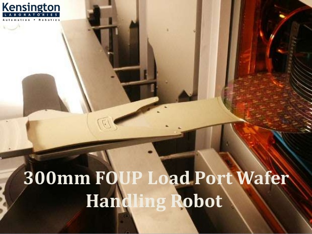
There is various thin wafer handling equipment available in the market to help you out with this issue. Many spin-coating applications need to be able to coat, develop, and rinse thinner and delicate substrates equally. There are many different types of substrates, but some of the more well-known ones are flexible polymer films, polyester, and metal foils. Safe handling of these delicate materials requires specially manufactured spin chucks and thin-wafer handling methods.
Additionally, the through-silicon via (TSV) technique for 3-D wafer stacking is moving up on the priority list of the microelectronics sector.
With this technology, the thickness of the substrate must be significantly reduced, and the handling requirements for each subsequent processing step become increasingly more complicated.
Issues Associated with Thin Wafer Handling Robots
Standard vacuum chucks, which supply vacuum through the spin chuck surface using a sequence of concentric circles and small-diameter perforated holes, can have a significant challenge to process engineers. These patterns unevenly distribute vacuum throughout the surface, leading to dimples, deflection, and/or, in the worst cases, cracking.
Special spin chucks are advised to properly contact thinner substrates without endangering delicate structures or compromising the homogeneity of the resulting film. Furthermore, these undesirable abnormalities will produce subpar film properties on the substrate. These sensitive films can be handled using a film frame support structure. However, abnormal chuck topography negatively impacts total thickness variation (TTV).
Types of Defects
Peeling
Peeling or particle contamination can happen in various ways throughout the semiconductor manufacturing process. As annealing steps are heated and cooled, the characteristics of the material change, causing a reduction in film adhesion. The edge, bevel, and apex are entirely encircled by the layers deposited during semiconductor manufacture. The stacks near the border can be partially removed by succeeding dry etches since they are not isotropic but not entirely around the bevel or apex region. As a result, the remaining stacked films may experience interfacial stress that hinders adequate adhesion. This may result in the formation of blisters, which may then develop larger due to thermal expansion. Other particles may be produced if the wafer manipulation breaks the blisters.
Micro Masking
Every high aspect ratio etches technique, including those used to create DRAM, NAND, and power devices, exhibits micro masking or needle-like flaws. If the etched part is disclosed at the bevel during the etch procedure, these flaws appear in the bevel region. The memory spot etch is non-selective to substrate in floating gate OPOP (Oxide-Poly Si-Oxide-Poly Si) gate first integration, and severe micro masking in the bevel region can occur during the memory hole, and slit etch. This particular flaw has been made worse by the scaling of 3D NAND storage.
During charge trap ONON (Oxide-Nitride-Oxide-Nitride) replacement gate integration, the silicon substrate is only etched with memory holes and slits. By carefully executing a bevel etch step, micro masking at the bevel can be decreased and prevented from occurring at the oxide-nitride layer.
The nitride is taken off, and tungsten is added during ONON integration. This nitride exhumes stage, especially if the previous high aspect ratio etch step produced micro masking in that area, can result in flaws at the bevel through wet undercut.
When technology is scaled back and complexity rises, the reducing-edge defect is a crucial component of raising yield. To increase wafer yield with the assistance of wafer handling equipment, it will be essential to comprehend edge flaws, including peeling and micro masking. These flaws can be reduced by including bevel etch and bevel clean procedures at crucial points in the process flow.


Comments
Post a Comment