Latest Trends in Semiconductor Fabrication to Look Out
There is a great need for silicon wafers, as it plays a critical role in emerging technologies. Looking at the coming future, the semiconductor market will definitely grow. Driving this growth will be the continuous rapid innovation of technologies that will digitalize the world. This digital era requires high-performance semiconductor devices.
Evolving Technologies are Advancing the Electronics Sector
As technology advances, the Semiconductor Wafers are becoming much thinner and more structurally complicated. Moreover, the latest technology demands complex ICs that are hard to create. To avoid defects or errors in the devices, the experts at the semiconductor industries are focused on providing the quality of equipment or products to handle everything precisely.
Wafer thinning/handling is one of the most critical things to be handled carefully. Many researchers & engineers have made great efforts to establish successful wafer handling robots. However, semiconductor manufacturers have often faced issues while finding new, more efficient ways to automate the handling of their wafers. The wafers come in a wide range of shapes & sizes; thus, they need different handling requirements. So, finding out the right handling solution may be a major challenge for the manufacturers.
Many companies have developed wafer edge grinding machines which is used in the semiconductor industry. This is where you need the experts. Whether you want automation solutions or are looking for the best wafer handling robots, choose the leading professionals who possess a deep understanding of wafer handling automation and factory integration requirements. In this way, you will get highly efficient wafer handling equipment that addresses all your project needs.
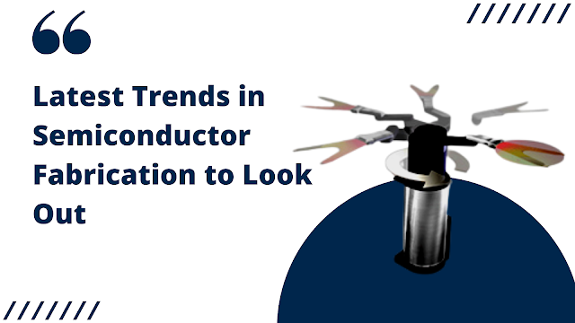
Reasons for Rising Demand for Wafer Handling Robots
The semiconductor manufacturing sector has a rising demand for wafer handling robots to deal with consumer electronics. These robots are used for manufacturing electronic parts, and it helps to bring improved results. Wafer handling robots are essential devices in integrated circuit manufacturing. They have high speed, excellent reliability, & great precision. These robots are best suited for automation as it gives rise to the precise and least contamination in wafer procedures.
The manufacturers design the diverse patterns of wafer handling robots to be used for the wafer handling process in different ways. The most famous wafer handling robots are SCARA wafer robots, frog leg robots, & four-bar linkage robots. It helps keep the contamination low during the wafer processing, which is the major demand of the manufacturing process.
Kensington Labs offers a full range of semiconductor services. They have a system which is highly configurable & customized in order to meet the exact specifications of the customers. All the experts at Kensington labs are highly skilled who dedicatedly work on the projects. The main mission of the experts is to provide the solution that facilitates the transfer of wafers safely and efficiently during the manufacturing process. Kensington professionals have a considerable contribution to the ongoing success of advanced manufacturers throughout the world.
Last Thoughts
Many professionals design and build reliable, industry-trusted semiconductor wafer handling systems around the globe. Looking for a dedicated business partner? Contact Kensington labs.


Comments
Post a Comment