How is Automation Technology Proving Beneficial for Semiconductor and Electronics Industry?
In this modern world, there is a great need for semiconductor devices. With the rising trends of the semiconductor industry, it is expected that there will be a tremendous transformation for most of the things involved today. Nowadays, the semiconductor & electronics manufacturing industry has a unique set of automation needs, including the mechatronic modules, which are specially designed for smooth motion. At the same time, the wafer handling or non-contact material is transported via the process chambers. Nowadays the Wafer Handling Automation equipment is quite trendy.
Though experts face many issues while working in the semiconductor industry, they still try to use the best techniques to handle everything efficiently. Presently the overall productivity of the semiconductor Fabrications is becoming much more dependent on the performance of the robotic systems, which are responsible for material handling within the front-end & back-end mini-environments.
The production of microelectronic ICs is one of the most complicated manufacturing environments in the industrial world. The major unit operations like fabrication processes, metrology, material handling as well as others were performed manually. However, with the rapid change in technological trends and modernization, these unit operations have been changed to automated control, which helps remove the need for human beings in the fab environment. As the process technology has evolved to the point where low to zero contamination levels have become the norm in the fab environments. In order to perform certain contaminants in the fab lab, there is still a need for the staff within the cleanroom.
With time, there is much improvement in contamination control as it is nowadays become more dependent on the automation within the fab. In the semiconductor industry, professionals use advanced devices to manufacture the right equipment as the industry need. The typical parameters which must be considered in any semiconductor manufacturing automation scheme consist of:
- Message sequencing standards between different tools& the host computer
- Engineering review & then control
- Manual override
- Wafer cassette identification
- Recipe ID & recipe body check
- One has to Load/unload port design
- Carefully handling the materials
- Process control is the main part
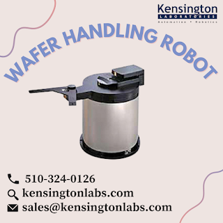
Kensington Laboratories, LLC has designed and manufactured innovative automation & precision motion control solutions for various industrial, scientific & academic applications. They are known for delivering innovative & robust technical solutions, wafer handling robots as well as precision stages.
About us:
Kensington is known as one of the best suppliers, which will surely meet your industrial needs. The professionals use high-end technology to design the industrial equipment. The unmatched feature of the Kensington robots & stages is the Zero Backlash design that offers precise positioning & improved repeatability. Kensington's abs have a long history of innovation and reliability in wafer handling robots & precision motion control.

Source Url:- https://kensingtonlabs.mystrikingly.com/blog/how-is-automation-technology-proving-beneficial-for-semiconductor-and


Comments
Post a Comment