The Detailed Guide to know about the AMAT Robot and Wafer Front End
Do you know that the semiconductor production process is divided into the following sequential processes, such as front-end and back-end production? The operations further indulge both complex and sophisticated steps. Primarily the wafer front end production was mainly referred to as wafer fabrication, whereas the back end production assembly and testing of the separate semiconductor devices.
When the front-end production process gets completed, the wafers are then conveyed to an assembly facility to curb the chip, assist integration into the electronic systems, confine the electrical interference and facilitate the binge of the heat from the devices.
The semiconductor back-end production has a consignment production form that is based on the several orders of many customers. If we talk in other words, the back-end companies build the final product with the help of the non-defective dies i.e., picked up from the wafer conveyed from the front-end production and lastly delivers the ultimate products within the due dates. If we go after discovering semiconductor die, it can be done through the EDS, electrical die sorting test mainly in the front-end production. Further, it checks whether the individual dies on a wafer and makes the way to reach the quality level or the individuals' die is repairable. It also tells in detail about the non-repairable chips which proceed to the next step. When this specific test got completed, the defectiveness and its opposed information are filled and passed on to the back-end process based on the information that only non-defective dies are made up into the final product.
Detailed view:
The following figure draws the semiconductor back-end processes. The initial process of the semiconductor back-end production is known as the back grinding (polishing) process, which sharpens the wafer's backside without a circuit. Its second process indulges the sawing process that cuts and separates the wafer passed via the back grinding process with the high-speed spinning diamond blade. Before implementing the wafer sawing process, the backside of the wafer.
Previously executing the wafer sawing process, the backside of the wafer is taped to dies the dust being dispersed during the wafer sawing procedure. Afterward, the wafer is cut into a different semiconductor chip. The die connect process is to append the non-damaged passes created from the wafer sawing procedure to the lead outline cushion of the strip and to empower the wire holding. Mainly, the quantity of the wafer sawing gear is more noteworthy than that of the pass on append hardware, and the wafer sawing process takes less time than the dies the die connects to the process. The wire bonding process associates the individual semiconductor chip to a circuit board by fixing the die pad of a chip to the leading edge of the strip. It utilizes programmed machines known as wire bonders and a metallic gadget, for example, aluminum or gold wires. Through the wire holding process, the leads on the lead outline are associated with the info and yield terminals on the semiconductor chip.
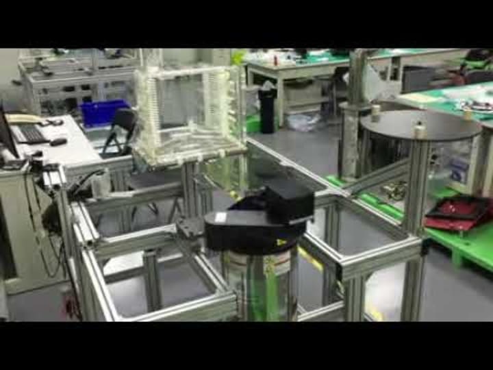
Jumping on the AMAT Robot:
The term 'AMAT' is known as the applied materials. The AMAT (applied materials) robot is the robotized programming, hardware, equipment, advanced by global organizations to utilize the item in several services. Examples include electronic-based coordinated chips, TVs, cell phones, sun oriented items, and so on.
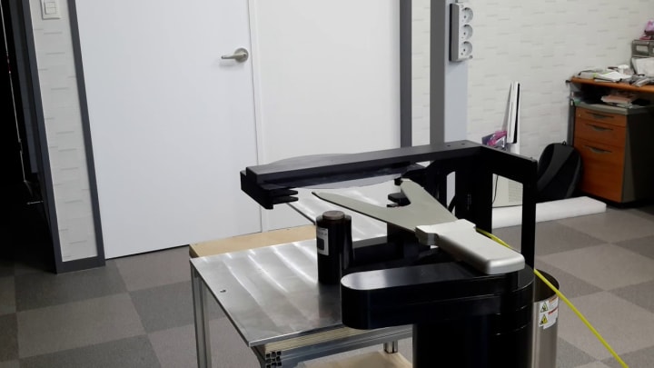
There are many viewpoints regarding the rules of the environmental wafer, applying robotics that incorporates appropriate materials, clean drive trains, and the surface completions. There are some major materials for the apply robotics, which will reduce the contamination of the particle from the contact and resistance. These include such materials for parts, coatings, material surfaces, oils, and various other segments. Next, the material incorporates stainless steel, aluminum, plastics, and many other components. The stainless steel is the most utilized for the unique moving parts, for instance, lead screws and orientation and little parts, such as screws and washers. It likewise includes the parts which are exposed to the vacuum and the critical situations.
Regarding purchasing the wafer handling AMAT Robot, Wafer Front End SCARA robots from the provider, most shoppers get bewildered because of the expansive rundown that is arranged on the digitized platform. Here is the big brand name Kensington Laboratories that fulfills the clients' major needs and attempt consistently to provide them the wide and best scope of items from ADOs, end-effectors, and wafer handling robots at the most moderate rate. Regardless of whether you are worried about the current frameworks' stage fixing, the designers of this firm would never let you feel disappointed. Thus, before even thinking about other brands, you can consult us to structure your custom products to accomplish automatic and unique outcomes.


Comments
Post a Comment