Basic Guide to Semiconductor Technology
Every month systems are producing more complex chips at the same price with reliable and economical automated solutions. It is important to be aware of the availability of semiconductors manufacturers and electronic components worldwide when you are into implementing several electronic functions. Most of the wafer front end and back-end manufacturing processes use the MOS technology in the majority of the ICs.
In an electric circuit, the semiconductor chip has many components wired on a semiconductor wafer. The components are patterned on a photomask (reticle) using a computer and in the manufacturing process are projected onto a semiconductor wafer.
Electronic circuits are formed with transistors in the IC manufacturing process on the surface of a silicon crystal wafer.
Wafer Processing
Semiconductor devices are completed either through the front-end process or the back-end process.
The semiconductor devices are used in many products like cars, personal computers, and smartphones that we use in everyday life. A semiconductor has the properties of a conductor as well as an insulator.
It conducts electricity under certain circumstances, and the conductance of a semiconductor depends on many factors. Current or voltage is applied to the intensity of irradiation by infrared (IR), ultraviolet (UV), X rays, and many other ways. The semiconductor has electrical conductivity greater than an insulator but less than a conductor.
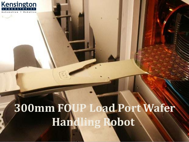
Kensington Labs has been delivering innovative and robust technical solutions to meet the demands of this industry. Wafer handling automation robots, precision stages, and integrated stages are specifically designed to make reliable systems with fine resolution capabilities.
Kensington is a leading supplier of the systems combined with nanometer-scale-precision with the robust performance for long operational life and low cost of the system. Kensington robots and wafer stage are known for enhanced repeatability and precise positioning.
The innovation and reliability in wafer handling robots have served a wide range of industries in major sectors with the latest technology and enhanced product lifetimes. There is a legacy of applications supported for the mature markets and the emerging markets.
Tips to Maximize equipment ROI
Kensington customers get equipment with latest technological innovation that operates for life. The proper analysis of wafer handling robots and precision stages has shown great results and a high return on investment in a short-term. All the products are well supported with spare parts, refurbishments, and repairs to help the customers make most of the customer capital expense.


Comments
Post a Comment