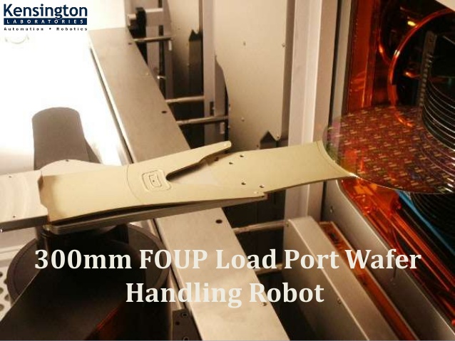
Semiconductor Manufacturing Process
Before producing an integrated circuit, a semiconductor
wafer goes through a wide range of processes steps. The key steps are Physical
Vapor Deposition (PVD) and Chemical Vapor Deposition (CVD), photolithography,
Rapid Thermal Processing (RTP), Plasma Etch, and Chemical-Mechanical
Planarization (CMP). For many years the standard practice to perform these
steps was to do so in batches on many wafers at a time so that a large number
of identical chips can be produced at the same time. When the demand for
smaller critical dimensions (CD) of the devices on the chip is increased and to
make the production process flexible, the makers went for integrated circuits.
Wafer fabrication comes under Wafer front end.
OVERVIEW OF TYPICAL WAFER PROCESSING EQUIPMENT
The wafer processing equipment is not produced in a single
step, there are many process steps which are necessary to produce a ULSI the circuit on a wafer. The physical processes are organized into groups that
correspond to the type of equipment that is beneficial to perform the specific
process.
The control engineer who is responsible for controlling the
processing equipment, the main issues can be summarized with the following five
questions:
- What are the processes involved (physics)?
- What are the actuators (inputs)?
- What sensors are available (outputs)? 4. What are the performance metrics?
- What are the uncertainties and disturbances?
CONTROL OF SEMICONDUCTOR PROCESSES
There are three components of the controller; the planner,
the regulator, and the estimator. The feedback controller has a regulator and
the estimator. The task of the planner is to translate the desired product
characteristics into nominal or an ideal set of process inputs and reference
signals. According to the type of the process, the inputs can be constant or
can follow a complex time history.
If the model and the planner are perfect and there are no
process disturbances, the planner is all that is required. But in the real
world, this is not possible, there are problems which arise out of the blue.
Thus, the regulator comes in handy. The regulator performs the important task
of minimizing the differences between uses the difference between the product
characteristics and the ideal product requirement. The feedback controller
computes the corrections to the nominal process inputs computed by the planner.
Together, the planner and the regulator make the model-based control portion of
the solution. The complications don’t stop here, in many cases it is not
possible to evaluate the relevant product characteristics in-situ either
because the sensor is not invented or because the whole process is way too
expensive. Thus, a model of the process conditions is used by the estimator.
The estimator infers the critical variables from the sensed variables.
Conclusion
The semiconductor manufacturing process is a complex task,
there are many issues which are inevitable. These issues can be minimized with
the help of expert minds of men and machines. In semiconductor equipment, precision stage repair is required
so that tasks don’t halt and there is no loss of productivity.


Comments
Post a Comment