Optimizing Throughput and Accuracy: Advanced Wafer Automation Techniques
Throughput and accuracy are the two most important factors in the fiercely competitive field of semiconductor production. Accuracy makes sure that the wafers match the industry's strict quality requirements, while throughput defines how many wafers your facility can create in a given amount of time. Wafer automation and sophisticated wafer cassette mapping techniques are useful in this situation.
What is Wafer Automation?
Using specialized robots, equipment, and software to handle and process semiconductor wafers throughout their intricate manufacturing process is known as wafer automation. This has numerous significant benefits over physical labor as it substitutes it at various stages of the process:
Increased Throughput:
Robots and automated systems can operate continuously, significantly boosting the speed of wafer processing.
Enhanced Precision:
Automation reduces the possibility of human mistake, avoiding damage such as scratches or contamination while maintaining proper handling.
Improved Safety:
Semiconductor production may include hazardous chemicals and procedures; automation decreases human exposure to these dangers.
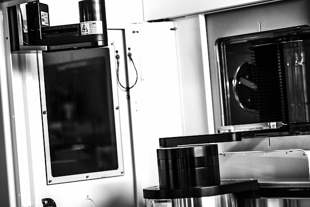
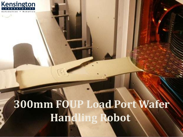
Wafer automation frequently involves robotic wafer handling systems, automated material handling systems (AMHS) for transporting wafer cassettes, and advanced sensors for process monitoring. It often integrates closely with wafer cassette mapping to ensure precision and tracking during movement and processing.
Advanced Techniques in Wafer Automation
Semiconductor manufacturing demands constant innovation to maximize throughput and precision. This drive has led to remarkable advancements in wafer automation. Here are a few cutting-edge techniques transforming the industry:
Robotic Wafer Handling:
Cleanroom robots are now a staple, delicately handling wafers to eliminate human error and contamination risks. Their speed and precision significantly increase throughput.
Automated Material Handling Systems (AMHS):
These systems use overhead transport, conveyors, or even autonomous vehicles to move wafer cassettes between stations without delay. AMHS optimizes efficiency and reduces manual transport.
Sensor-Driven Process Control:
Wafer automation now includes real-time sensor feedback. This enables intelligent process adjustments for optimal conditions, enhancing accuracy and yield.
Integrated Wafer Cassette Mapping:
Mapping systems within automation ensure accurate tracking and quality control. By identifying problematic wafers early, it prevents wasted resources.
These advanced techniques in wafer automation are driving semiconductor fabrication to new heights of efficiency and accuracy. Continued innovation in this area promises to revolutionize future chip manufacturing.
The Importance of Wafer Cassette Mapping
Wafer cassette mapping is a deceptively simple yet crucial element of modern semiconductor manufacturing. It involves assigning a unique identifier and position to each wafer housed within a cassette. Here's why mapping is so important:
Precision Tracking:
Mapping allows for accurate tracking throughout the complex fabrication process, which is crucial when processes involve hundreds of steps.
Quality Control:
Mapping helps identify defects early – misalignments, scratches, or contamination – preventing those wafers from further costly processing.
Optimization Insights:
Wafer map data reveals patterns that can pinpoint areas for process improvement, boosting yield and reducing waste.
Automation Compatibility:
Accurate mapping is essential for wafer automation systems to function correctly, guide robots, and ensure wafers are handled with the necessary precision.
Wafer cassette mapping, though often overlooked, provides the foundation for efficiency, quality control, and a streamlined production flow within semiconductor manufacturing.
Bringing it All Together
The synergy between wafer automation and accurate wafer cassette mapping is essential for pushing the boundaries of semiconductor manufacturing. By maximizing the speed, precision, and control over wafer processing, these technologies help:
- Increase production yields
- Reduce defects and waste
- Boost overall profitability
As wafer automation and mapping techniques advance, semiconductor manufacturers will have more control over their operations. This, in turn, will be critical in developing ever tiny, powerful, and efficient integrated circuits to power the world's electronic gadgets


Comments
Post a Comment