Posts

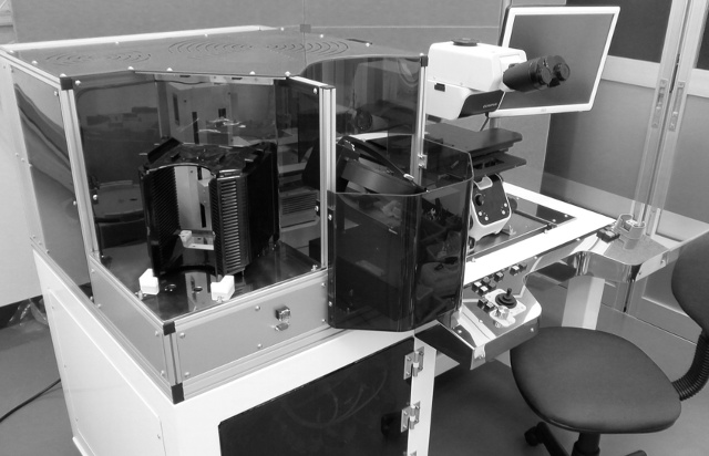
Optimizing Throughput and Accuracy: Advanced Wafer Automation Techniques

Image
Throughput and accuracy are the two most important factors in the fiercely competitive field of semiconductor production. Accuracy makes sure that the wafers match the industry's strict quality requirements, while throughput defines how many wafers your facility can create in a given amount of time. Wafer automation and sophisticated wafer cassette mapping techniques are useful in this situation.  What is Wafer Automation?  Using specialized robots, equipment, and software to handle and process semiconductor wafers throughout their intricate manufacturing process is known as wafer automation. This has numerous significant benefits over physical labor as it substitutes it at various stages of the process:  Increased Throughput:  Robots and automated systems can operate continuously, significantly boosting the speed of wafer processing.  Enhanced Precision:  Automation reduces the possibility of human mistake, avoiding damage such as scratches or contamination while maintaining prop

Optimizing AMAT Robot Performance: A Guide to Precision Motion Control Techniques

Image
Precision is critical for success in the highly competitive and challenging sector of semiconductor production. Applied Materials (AMAT) robots are a hallmark of this industry, noted for their dependability and ability to handle delicate wafers with pinpoint precision. Even the best robotic systems might benefit from tuning to guarantee they continue to function at optimal levels.  This article looks into crucial precision motion control techniques for maximizing the capabilities of your AMAT robot.  Understanding Precision Motion Control  Precision motion control lies at the heart of manufacturing processes that demand accuracy and repeatability - nowhere more so than in semiconductor production where AMAT robots excel. This form of motion control goes beyond simple movement. Here's what it entails:  Accuracy: The ability of the robot to reach the exact intended position within tight tolerances, often measured in microns.  Repeatability: The robot's capacity to consistently

Wafer Cassette Mapping: The Essentials for Semiconductor Manufacturing

Image
In the complex world of semiconductor production, efficiency and precision are not just desirable outcomes, but rather requirements. Every tiny transistor that is etched into a silicon wafer needs to be precise since any mistake might result in expensive losses.  Here's where wafer cassette mapping comes into play: it's the foundation of quality control that protects yield and guarantees the creation of perfect electronics.   What is Wafer Cassette Mapping?  Let's begin by envisioning the procedure. Semiconductor manufacturing starts off with pristine silicon wafers, which are tiny, round discs that serve as the basis for integrated circuits. These wafers are housed in protective containers called cassettes. Wafer cassette mapping is the process of meticulously analyzing each wafer within a cassette, pinpointing defects, identifying performance variations, and classifying the individual dies. This mapping process generates a visual representation of the wafer – a "map

Precision and Speed: Optimizing Wafer Automation with Advanced EFEMs

Image
Semiconductor manufacturing – the backbone of the modern digital world – operates on a microscopic scale. The slightest deviation in the fabrication of delicate silicon wafers can compromise the performance and yield of countless electronic devices.   As the insatiable demand for greater computing power and smaller form factors intensifies, optimizing speed and absolute precision during wafer handling has become critical. Let's explore how advanced EFEMs are pushing the boundaries of precision and speed in wafer automation .  What is an EFEM?  An EFEM (Equipment Front-End Module) is the entrance point for wafers into advanced semiconductor manufacturing machines. It functions as a tightly regulated mini-environment, protecting delicate wafers from contamination while maintaining ideal atmospheric conditions during loading, unloading, and temporary storage.  EFEMs work in perfect synergy with wafer-handling robots or automated material handling systems (AMHS) ensuring a seamless and

Efficiency in Motion: Wafer Automation with AMAT Robot

Image
In today's ever-evolving semiconductor fabricating era, exactness, speed, and proficiency are fundamental. Not to mention, AMAT Robot combines a high-performance robotization program which is one of the foremost inventive innovations within the industry. Here, in this post, we'll shed light on how these cutting-edge innovations are revolutionizing semiconductor fabricating and driving the industry forward.   The Semiconductor Manufacturing Challenge    Semiconductor manufacture could be a complicated handle that requires exactness at all stages. From wafer stacking and emptying to review and pressing, each prepare must be completed immaculately. Truly, these operations were as often as possible labor-intensive, time-consuming, and vulnerable to human botch. Find the world of AMAT Robot and Wafer automation.   Precision and Efficiency in AMAT Robots    Wafer-handling robots are the mainstays of semiconductor production. These specialist robots are meant to handle semiconductor

Efficiency Unleashed: The Power of Wafer Automation!

Image
Every faultless execution or cutting-edge technological development conceals an entire realm of precision and ingenuity that is frequently unavailable to the general audience. The undiscovered treasures of semiconductor manufacturing are the labs dedicated to wafer automation and stage repair . This article will examine the fascinating features of these particular labs, where expertise and advances in technology combine to create immaculate environments and progress within the semiconductor industry.    Phases of Creation and Replication: The Alchemy of Substances    Professional stage repair services are often not exposed to threats and are a more reliable option, especially for critical applications where precision is non-negotiable. Like wizards, the skilled workers fuse elements and wisdom to create fresh possibilities for semiconductor manufacturing. Whether it's by restoring modern semiconductor companies or reconstructing antique instruments, something extraordinary occurs w

Unveiling the Wonders of Kensington Controllers and Wafer Handling!

Image
There is no denying the fact that Wafer handling and Kensington controller are two hidden icons that are crucial to the constantly changing fields of precision engineering and technology. These humble parts are the foundation of state-of-the-art systems, quietly changing the way we use technology. Let's investigate the world of these technical wonders and discover all the advantages they provide.   Kensington Controllers: A Symphony of Control and Precision  Kensington controllers' inventiveness is the key to flawless user experiences. These often-ignored gadgets are the maestros arranging the control symphony in a variety of electronic applications. a Kensington controller offers an easy-to-use interface that improves user engagement with unprecedented precision on a variety of devices, including smart gadgets and arcade machines.   Enhanced Ergonomics for Unmatched Comfort   The dedication of a Kensington controller to ergonomics is one of their most notable features. These